Matrix type printed circuit board for semiconductor packages

a semiconductor and printed circuit board technology, applied in the direction of electrical equipment, electrical contruction details, basic electric elements, etc., can solve the problems of low productivity, limitation on the reduction of manufacturing costs, and large limitation on the number of semiconductor packages fabricated from one pcb strip, so as to improve the efficiency of the resin encapsulation molding process

Inactive Publication Date: 2003-06-17
AMKOR TECH SINGAPORE HLDG PTE LTD
View PDF8 Cites 32 Cited by
  • Summary
  • Abstract
  • Description
  • Claims
  • Application Information

AI Technical Summary

Benefits of technology

is to provide a matrix type PCB for semiconductor packages having a structure capable of allowing an increased number of PCB units to be simultaneously molded in a resin encapsulate molding process, thereby achieving a great improvement in the efficiency of the resin encapsulate molding process.

Problems solved by technology

However, the above mentioned conventional PCB strip 10' has a problem in that there is a great limitation on the number of semiconductor packages fabricated from one PCB strip.
Although active attempts have been made in a variety of fields associated with the fabrication of semiconductor packages to reduce the manufacturing costs, there is a limitation on the reduction of manufacturing costs insofar as the PCB strip 10' having the above mentioned structure is used.
The above mentioned PCB strip structure also involves a problem of a low productivity in that there is a great limitation on the number of PCB units processed per process in the fabrication of semiconductor packages.

Method used


Image

  • Matrix type printed circuit board for semiconductor packages
  • Matrix type printed circuit board for semiconductor packages
  • Matrix type printed circuit board for semiconductor packages

Examples


Embodiment Construction

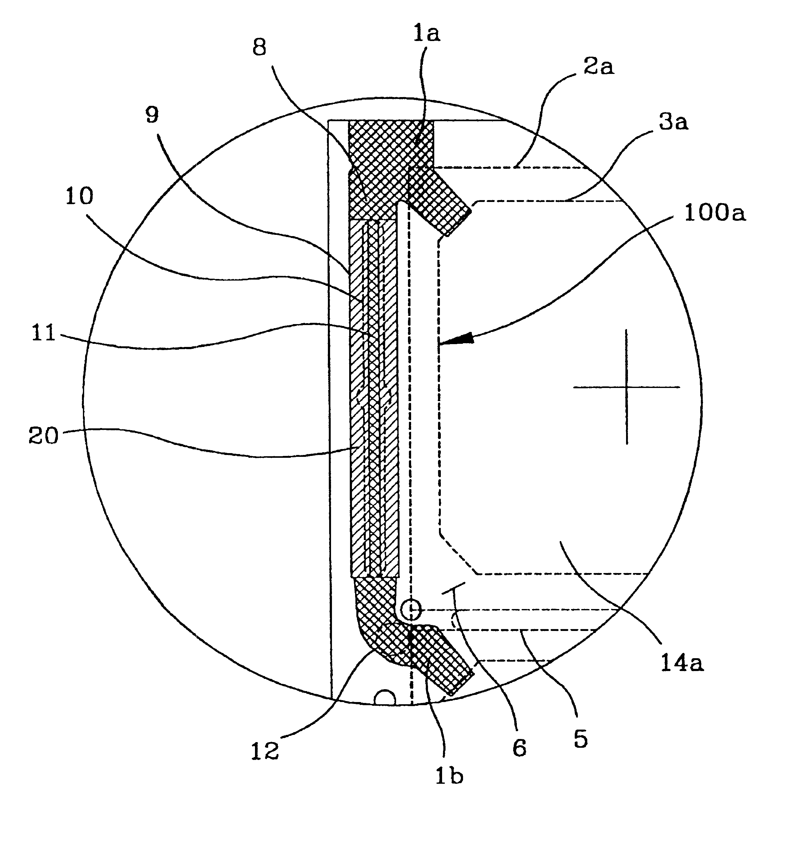
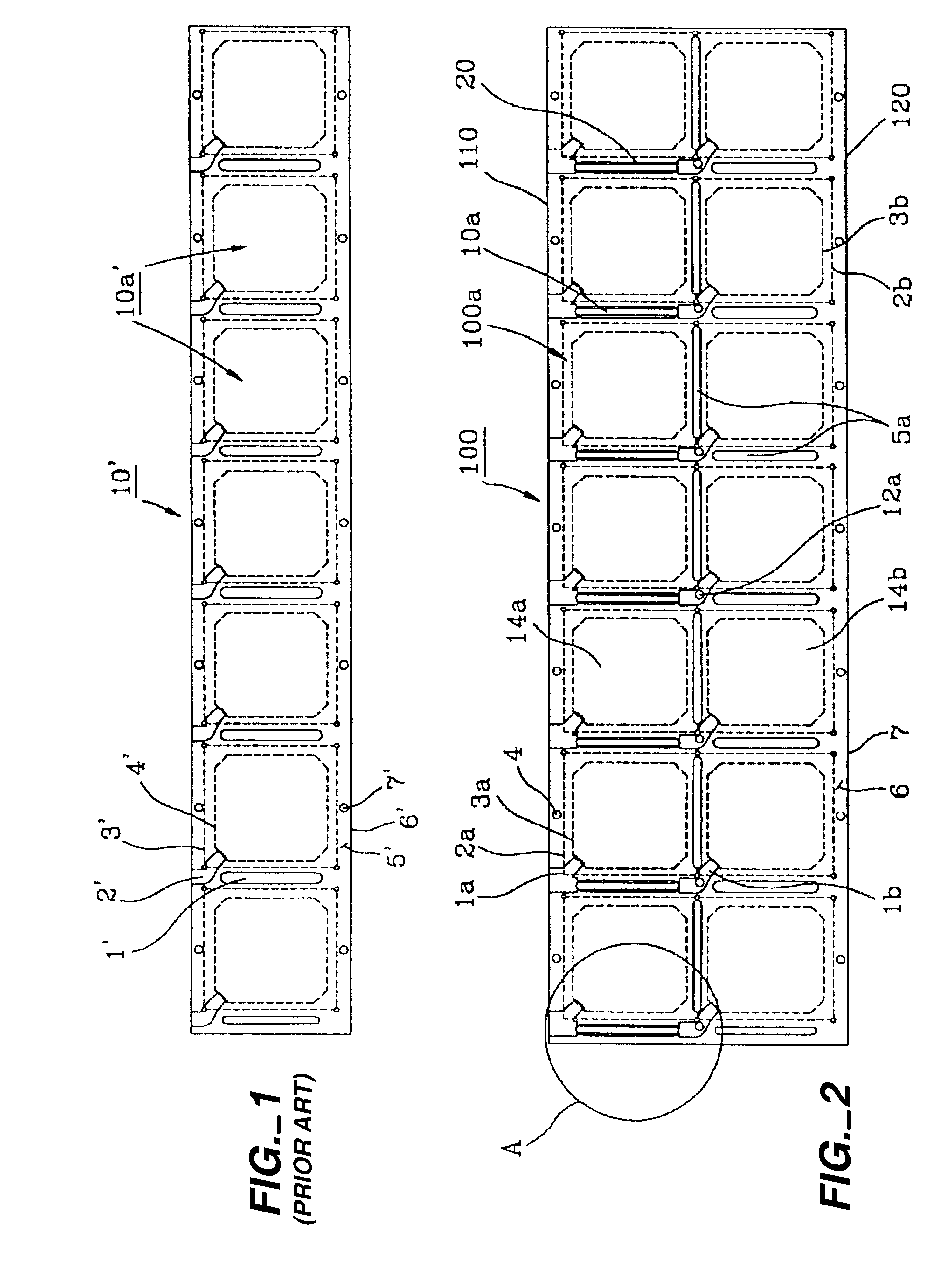
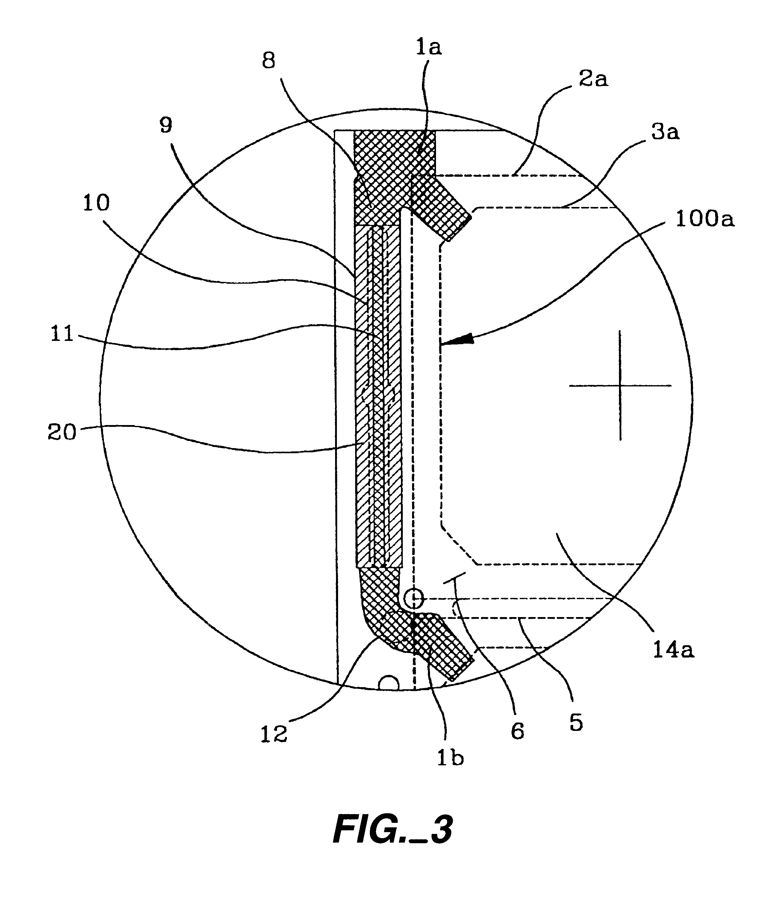
FIG. 2 is a schematic plan view illustrating a matrix type PCB according to an embodiment of the present invention. As shown in FIG. 2, the matrix type PCB, which is denoted by the reference numeral 100, is configured to have a plurality of PCB units 100a arranged in a matrix array having at least two rows. In the illustrated case, the PCB 100 has only two PCB unit rows 110 and 120. However, the present invention is not limited to the PCB having only two PCB unit rows. In accordance with the present invention, the PCB 100 may have three, four or more PCB unit rows in so far as a mold runner extends between adjacent mold runner gates of adjacent PCB unit rows.

As shown in FIG. 2, the PCB 100 includes a resin substrate 7 having a rectangular shape provided with two parallel longer edges and two parallel shorter edges. Although not shown, circuit patterns are formed on the upper surface or both the upper and lower surfaces of the resin substrate 7.

The circuit patterns have the form of r...


PUM


Abstract

Disclosed is a matrix type printed circuit board (PCB) for semiconductor packages having a structure including a plurality of PCB units arranged in a matrix array having at least two rows in such a fashion that the mold runner gates of adjacent PCB units respectively arranged in adjacent rows while being arranged in the same column communicate with each other by an integrate mold runner, thereby being capable of allowing an increased number of PCB units to be simultaneously processed in each process involved in the fabrication of semiconductor packages, so that a great improvement in productivity is achieved. In particular, it is possible to allow an increased number of PCB units to be simultaneously molded in a resin encapsulate molding process, thereby achieving a great improvement in the efficiency of the resin encapsulate molding process. Furthermore, surplus encapsulating resin materials cured in the mold runner gates and integrate mold runners can be easily and reliably removed in accordance with a degating and/or deculling process without a surface damage of the PCB. It is also possible to achieve an easy open/short circuit test for individual PCBs.

Description

1. Field of the InventionThe present invention relates to a method for reproducing a printed circuit board (PCB) for semiconductor packages, and more particularly to a matrix type PCB for semiconductor packages having a structure including a plurality of PCB units arranged in a matrix array having at least two rows in such a fashion that the mold runner gates of adjacent PCB units respectively arranged in adjacent rows while being arranged in the same column communicate with each other by an integrate mold runner, thereby being capable of allowing an increased number of PCB units to be simultaneously processed in each process involved in the fabrication of semiconductor packages, so that a great improvement in productivity is achieved.2. Description of the Prior ArtGenerally, a PCB is a circuit board adapted to transmit electrical signals from a semiconductor chip mounted thereon to an external unit and from the external unit to the semiconductor chip. Such a PCB is fabricated by la...

Claims


Application Information

Patent Timeline
Patent Type & Authority Patents(United States)
IPC IPC(8): H01L21/02H01L21/56H05K3/28H05K3/00H01L23/28
CPCH01L21/565H05K3/284H05K3/0052H01L2924/0002H01L2924/00H01L23/28
Inventor KIM, SUNGJIN
Owner AMKOR TECH SINGAPORE HLDG PTE LTD
Why Eureka
Try Eureka