Electro-optic electric field probe

a technology optical probes, applied in the field of electric field probes, can solve the problems of inability to image or probe internal devices of the integrated circuit, insufficient measurement of waveforms by conventional electronic measurement systems, and inability to test individual semiconductor devices

Inactive Publication Date: 2003-07-01
SOUTHWEST SCI
View PDF4 Cites 17 Cited by
  • Summary
  • Abstract
  • Description
  • Claims
  • Application Information

AI Technical Summary

Problems solved by technology

Conventional electronic measurement systems are no longer adequate to measure waveforms in the fastest electronic devices and integrated circuits.
These instruments do not function on centrosymmetric semiconductors such as silicon or germanium, however.
Unfortunately, such an approach cannot image or probe internal devices in the integrated circuit.
Also, such approaches can add parasitic capacitance to the device being probed which will skew any measurements.

Method used


Image

  • Electro-optic electric field probe
  • Electro-optic electric field probe
  • Electro-optic electric field probe

Examples


Embodiment Construction

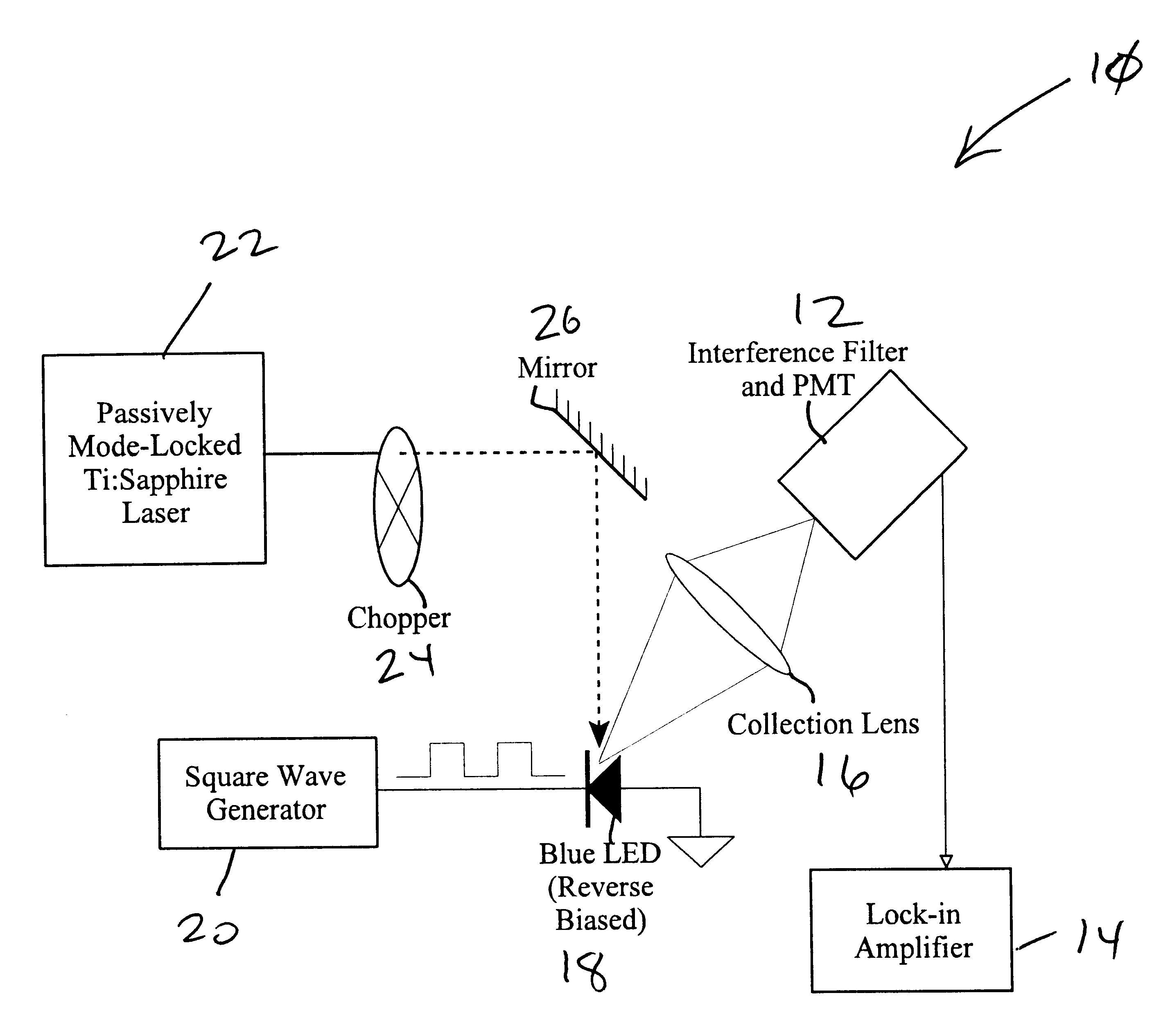
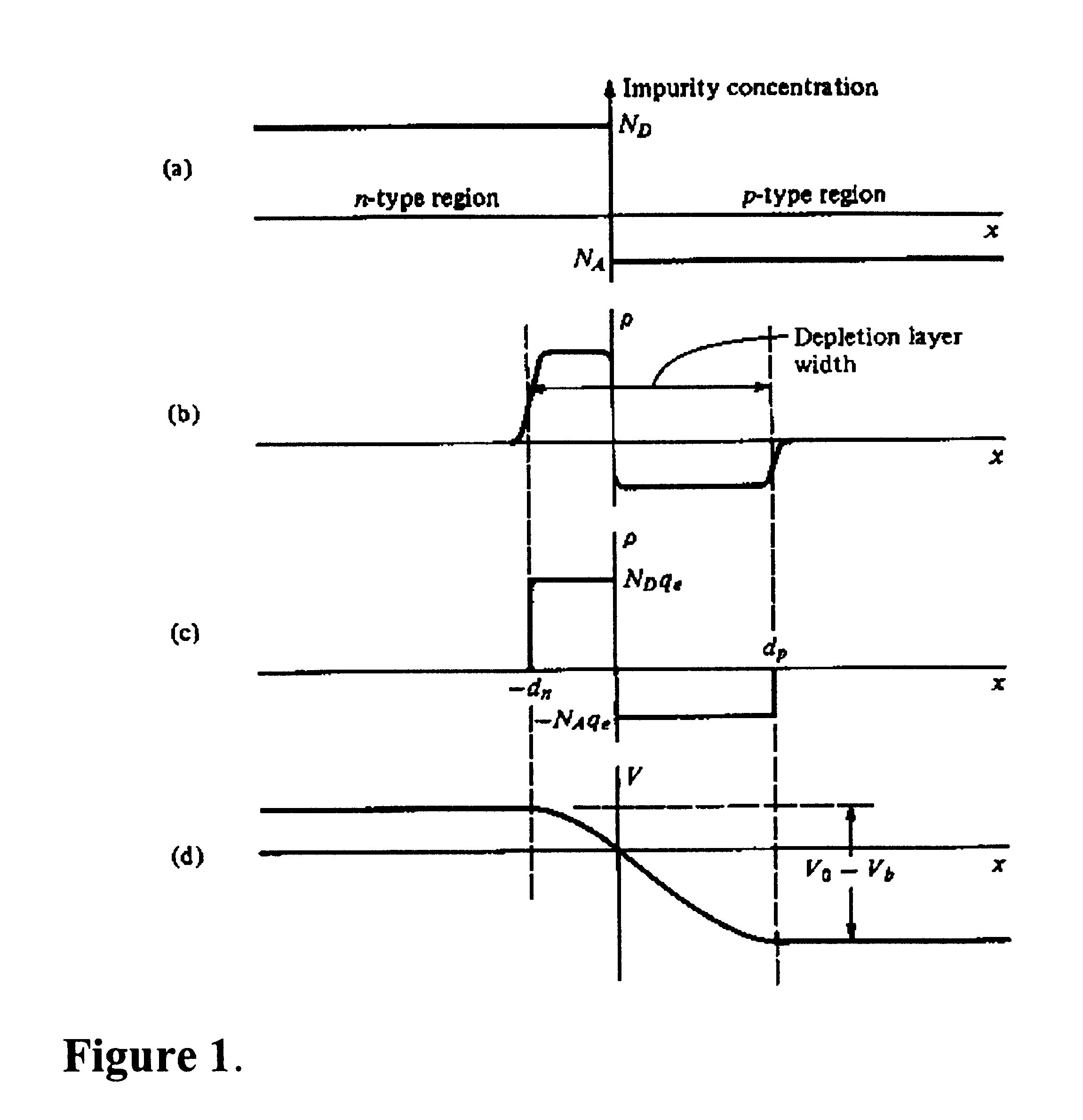
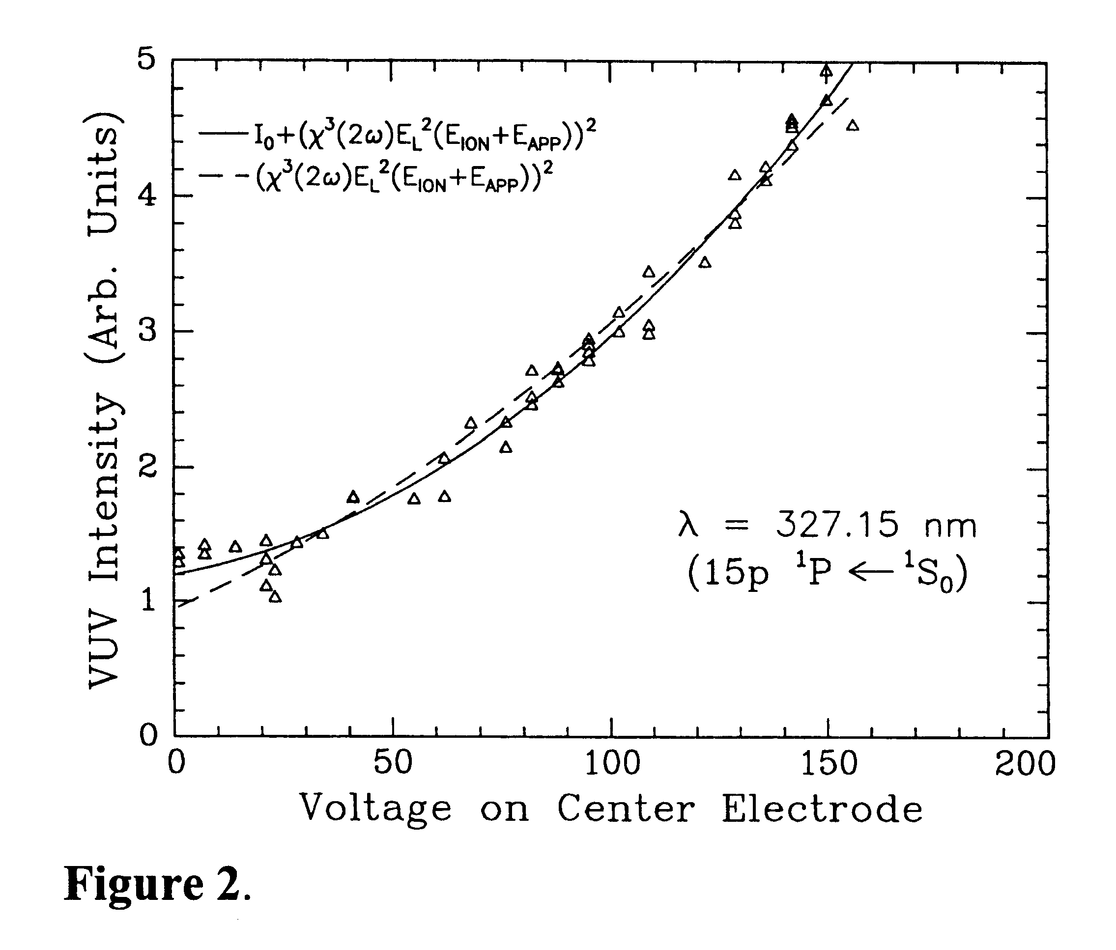
The present invention is of an electro-optic method and apparatus for probing electric fields, and hence waveforms, in integrated circuits noninvasively and without external probes. The inventive technique works on any semiconductor regardless of its crystal structure, and is useful for both imaging and single point detection without degradation of temporal resolution. Because the inventive technique is optically based, no parasitic capacitance is added to the device being measured. According to the present invention, a femtosecond laser probes the device to be measured; thus its temporal resolution is several orders of magnitude faster than the time resolution required to probe present devices. The inventive method is specific to only the depletion layer of the p-n junction or metal-semiconductor junction being probed. Other parts of the device are ignored. The optical nature of the technique of the present invention permits internal device structures of an integrated circuit to be...


PUM

PropertyMeasurementUnit
diameteraaaaaaaaaa
diameteraaaaaaaaaa
total energyaaaaaaaaaa

Abstract

A non-invasive electro-optic probe and probe method for probing electric fields in semiconductor devices comprising directing laser output at a semiconductor device to be probed employing a laser having an operating wavelength such that photon energy of a second harmonic wavelength of the operating wavelength is below the band gap of a semiconductor comprised by the semiconductor device and detecting second harmonic wavelength but not operating wavelength radiation from the semiconductor device.

Description

1. Field of the Invention (Technical Field)The present invention relates to electric field probes for high-speed integrated circuits and semiconductor devices.2. Background ArtNote that the following discussion refers to a number of publications by author(s) and year of publication, and that due to recent publication dates certain publications are not to be considered as prior art vis-a-vis the present invention. Discussion of such publications herein is given for more complete background and is not to be construed as an admission that such publications are prior art for patentability determination purposes.Operating speeds of electronic devices and integrated circuits (IC) are rapidly surpassing the capabilities of conventional electronic measurement instrumentation. Evaluation of fast semiconductor devices requires both high temporal resolution and the ability to probe internal points of an IC noninvasively. While optical methods promise ultrashort temporal resolution (.about.50 f...

Claims


Application Information

Patent Timeline
Patent Type & Authority Patents(United States)
IPC IPC(8): G01R31/28G01R31/311
CPCG01R31/311
Inventor KANE, DANIEL J.
Owner SOUTHWEST SCI
Why Eureka
Try Eureka