Semiconductor optical device with improved efficiency and output beam characteristics

a semiconductor laser and optical device technology, applied in the field of semiconductor lasers, can solve the problems of reducing the angular intensity profile of the optical radiation emitted by the semiconductor laser, affecting the effect of the p-side cladding, and reducing the efficiency of the semiconductor laser

Inactive Publication Date: 2003-07-29
SQUARE 1 BANK +1
View PDF9 Cites 30 Cited by
  • Summary
  • Abstract
  • Description
  • Claims
  • Application Information

AI Technical Summary

Problems solved by technology

However, for single-mode applications, such as coupling light into optical fibers, it is crucial that the angular intensity profile of the optical radiation emitted by the semiconductor laser remain nearly diffraction limited.
This loss is particularly large for the p-side cladding.
However, a broadened waveguide may cause adverse effects as well.
Consequently, the temperature sensitivity of the slope efficiency is deteriorated at high temperatures.
However, electron leakage current over the low doped cladding layer has been found to become significant with temperature, and render threshold current and slope efficiency highly temperature sensitive.
A fundamental disadvantage of this approach, however, is that the transverse optical mode is no longer a single lobed gaussian shape.
This distortion of the far field pattern significantly degrades device performance including reduced coupling efficiency of the laser to a single mode fiber.

Method used


Image

  • Semiconductor optical device with improved efficiency and output beam characteristics
  • Semiconductor optical device with improved efficiency and output beam characteristics
  • Semiconductor optical device with improved efficiency and output beam characteristics

Examples


Embodiment Construction

Reference will now be made in detail to presently preferred embodiments of the invention. Wherever possible, the same reference numbers will be used throughout the drawings to refer to the same or like parts.

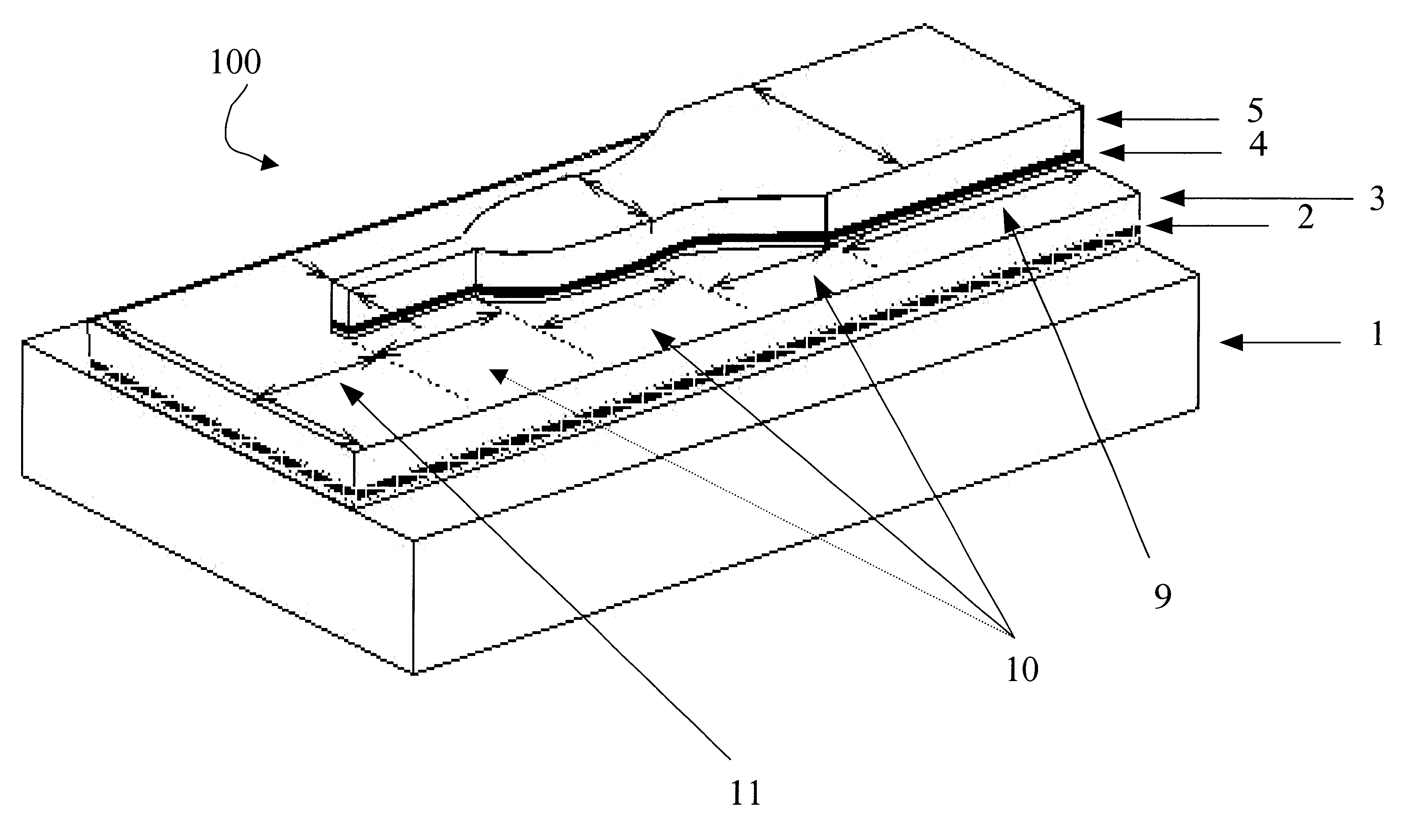
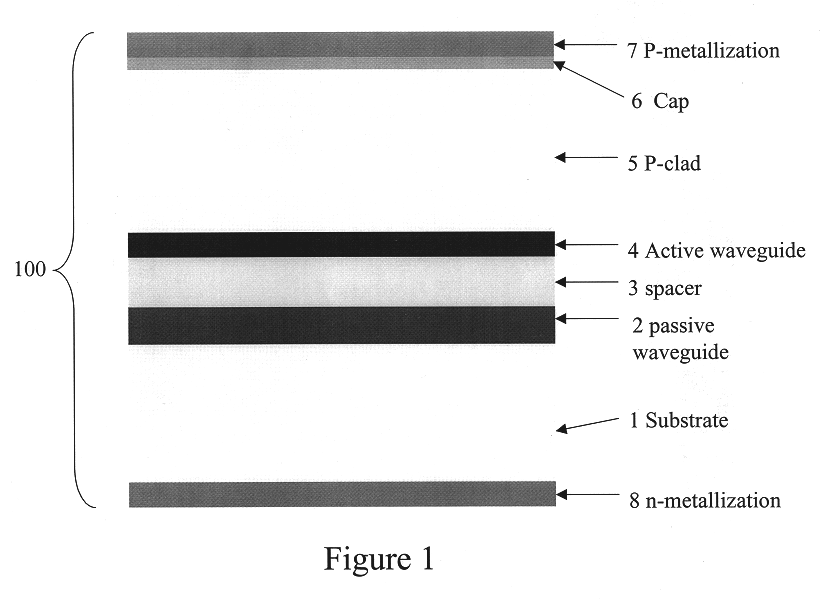
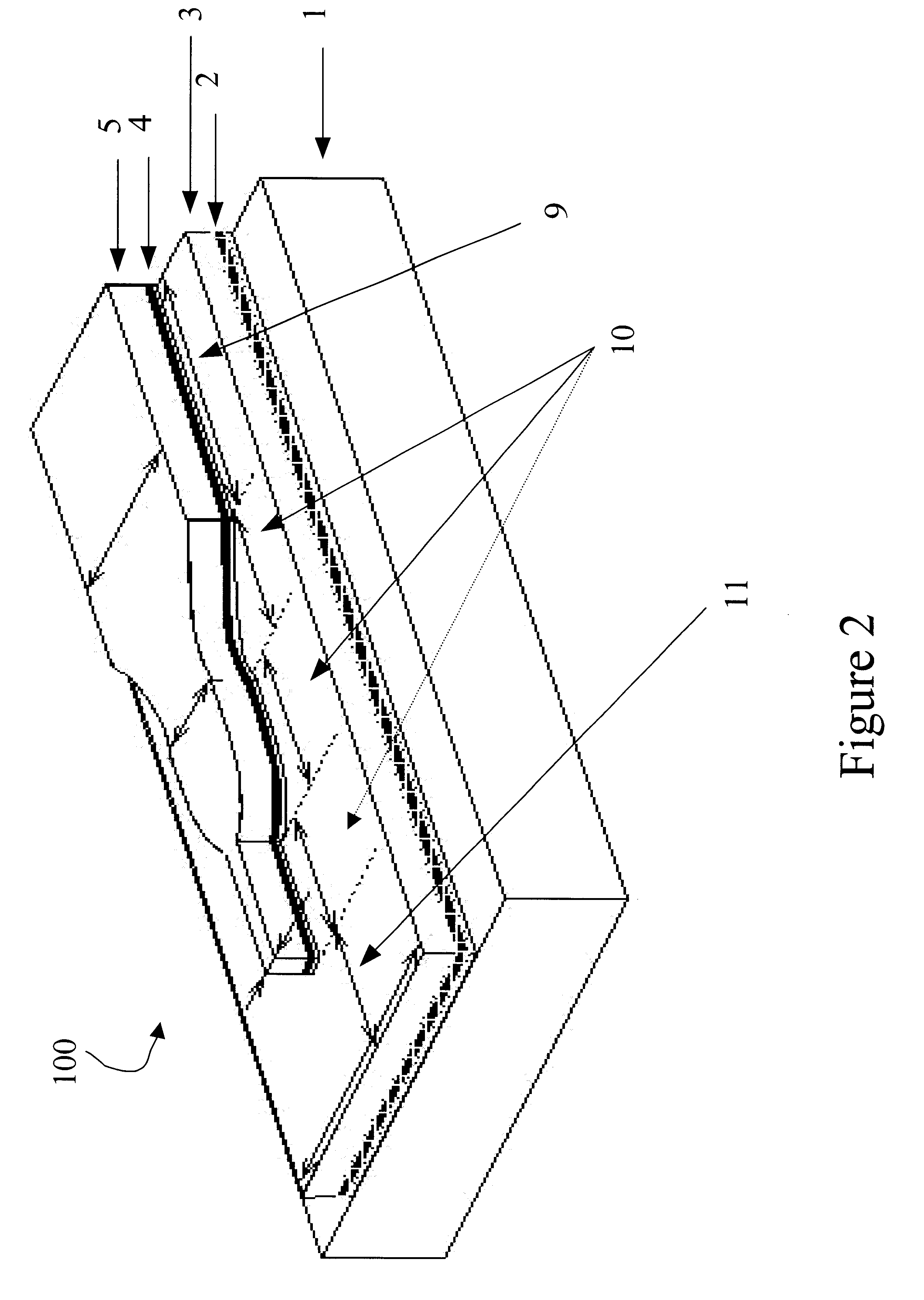
A semiconductor laser 100 according to a first embodiment of the present invention is shown in the cross-sectional view of FIG. 1, and the perspective view of FIG. 2. By way of example, other optical devices according to the present invention may include light emitting diodes (LED), semiconductor optical amplifiers, and other optical devices as would be readily apparent to one skilled in the art.

In this first embodiment, the semiconductor laser 100 comprises a gain section 9, a coupling section 10, and a passive section 11 which each may include multiple layers. These layers include a passive waveguide 2 and an active waveguide 4 separated by a spacer layer 3. Preferably, the passive waveguide 2 spans the length of the laser 100. As will be described later, the active waveguide ...


PUM


Abstract

An optical device is provided comprising a gain section adapted to emit radiation at a radiation wavelength, a coupling section adjacent to the gain section for transitioning radiation between an active waveguide and a passive waveguide, and a passive section adjacent to the coupling section supporting a single-lobed optical mode in the passive waveguide at the radiation wavelength. The passive waveguide has an index of refraction and dimension such that the confinement of the radiation within the active waveguide in the gain section is reduced.

Description

A. Field of the InventionThe invention relates generally to light emitting devices, more particularly, to semiconductor optical lasers having an improved design to reduce internal optical loss.B. Description of the Related ArtSemiconductor lasers are attractive sources for optical power generation because they are more efficient, smaller, and less expensive than other types of lasers. There are increasing applications for higher output power single-spatial-mode semiconductor lasers such as for pumping optical fiber amplifiers / lasers, optical wireless communications, optical fiber transmitters, and other laser applications. The output optical power from a semiconductor laser (P) is governed by a simple relationship: P=S.times.(I-I.sub.th). As the current (I) injected into the semiconductor laser is increased above the threshold current value (I.sub.th), the output power increases proportionally with a constant of proportionality S known as the slope efficiency. High power semiconduct...

Claims


Application Information

Patent Timeline
Patent Type & Authority Patents(United States)
IPC IPC(8): G02B6/122G02B6/12H01S5/22H01S5/10H01S5/00
CPCG02B6/1228G02B2006/12078G02B2006/12195H01S5/1014H01S5/1032H01S5/1064H01S5/22
Inventor SAINI, SIMARJEETHEIM, PETER J. S.
Owner SQUARE 1 BANK
Why Eureka
Try Eureka