Closed-grid bus architecture for wafer interconnect structure

a closed-grid bus and interconnect technology, applied in the direction of cross-talk/noise/interference reduction, individual semiconductor device testing, instruments, etc., can solve the problems of unsuitable interconnect structure for wafer-level tester interconnect, untested ic on each wafer, and distorted signal wave front of the daisy chain bus

Inactive Publication Date: 2003-08-05
FORMFACTOR INC
View PDF27 Cites 146 Cited by
  • Summary
  • Abstract
  • Description
  • Claims
  • Application Information

AI Technical Summary

Problems solved by technology

A long-daisy chain bus can also severely distort the signal wave front as it passes from node-to-node; the last node on the bus will see substantially slower rise time than the first.
Since an interconnect structure for a wafer-level tester would have a large number buses formed by small traces, since each bus would include a large number of nodes on each bus, and since each bus would be implemented by small traces, there would be many places on the bus were a fault could occur, and any one fault would render the interconnect structure unsuitable for use in a wafer-level tester interconnect system since several ICs on each wafer would be untestable.
However even a single open circuit fault would none-the-less render an interconnect structure employing a star bus unsuitable in a wafer-testing because it would mean that one IC on each wafer would be untes...

Method used


Image

  • Closed-grid bus architecture for wafer interconnect structure
  • Closed-grid bus architecture for wafer interconnect structure
  • Closed-grid bus architecture for wafer interconnect structure

Examples


example pcb layout

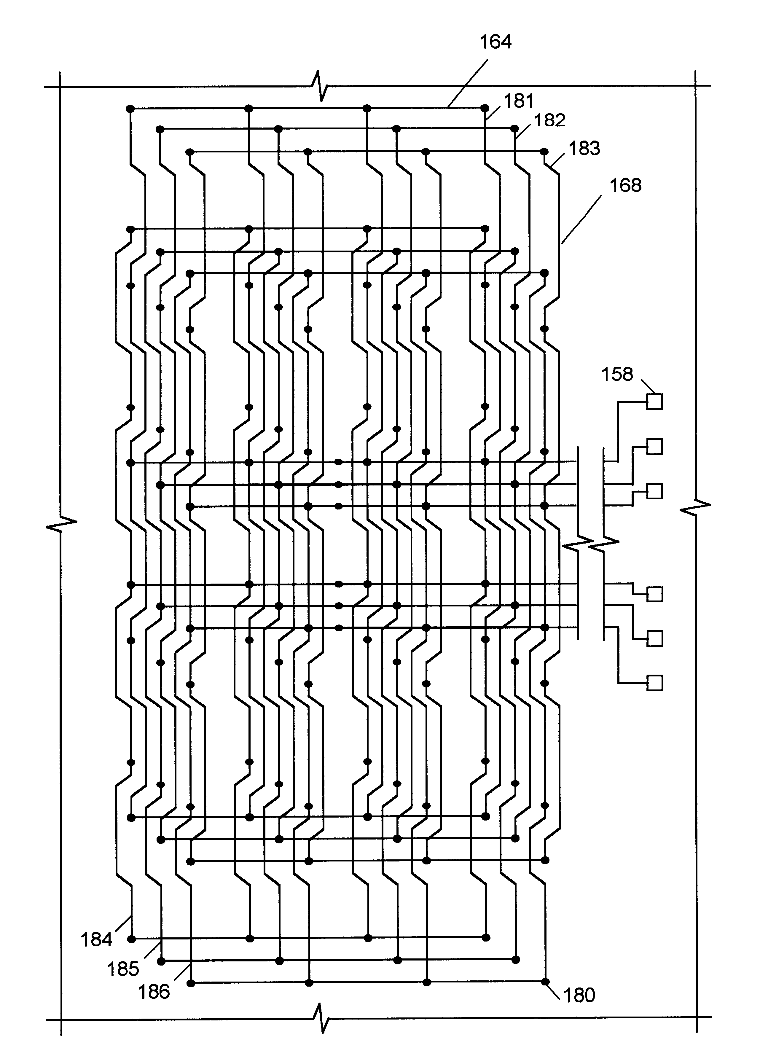
FIG. 13 is a simplified plan view of a portion of an example semiconductor wafer 150 containing a 4.times.5 array of ICs 152, each IC having 6 pads 154. FIGS. 14-19 describe a layout for a PCB within an interconnect structure that will provide six closed-grid buses, each linking a separate set of twenty corresponding I / O pads 154 of all twenty ICs 152 to a separate tester channel.

FIG. 14 is a simplified (not to scale) plan view of a portion of the top layer 121 of the PCB. A set of six conductive pads 158 are arranged on layer 156 to receive pogo pin or coaxial conductors from the six channels. A set of traces 160, suitably of similar length, link pads 158 to a set of six vias 162 passing downward to a next lower layer of the PCB.

FIG. 15 is a simplified (not to scale) plan view of a portion of that next lower layer 122. Layer 122 includes a set of eighteen traces 164 extending along "east / west" axes. The six vias 162 from top layer 121 are each linked to a separate one of traces 164...


PUM

PropertyMeasurementUnit
Electrical conductoraaaaaaaaaa

Abstract

An interconnect structure employs a closed-grid bus to link an integrated circuit tester channel to an array of input/output (I/O) pads on a semiconductor wafer so that the tester channel can concurrently communicate with all of the I/O pads. The interconnect structure includes a circuit board implementing an array of bus nodes, each corresponding to a separate one of the I/O pads. The circuit board includes at least two layers. Traces mounted on a first layer form a set of first daisy-chain buses, each linking all bus nodes of a separate row of the bus node array. Traces mounted on a second circuit board layer form a set of second daisy-chain buses, each linking all bus nodes of a separate column of the bus node array. Vias and other circuit board interconnect ends of the first and second daisy-chain buses so that they form the closed-grid bus. Each bus node is connected though a separate isolation resistor to a separate contact pad mounted on a surface of the circuit board. A set of spring contacts or probes link each contact pad to a separate one of the I/O pads on the wafer.

Description

1. Field of the InventionThe present invention relates in general to an interconnect structure for providing signal paths between test equipment and contact pads on a semiconductor wafer, and in particular to a wafer interconnect structure employing a closed-grid bus to distribute signals to several integrated circuit devices under test.2. Description of Related ArtIn many applications microstrip or stripline traces convey a logic signal from a single source to many nodes on a printed circuit board (PCB). For example traces on a motherboard commonly distribute data, address and control lines of computer buses to sockets holding daughterboards, or traces on a PCB may distribute a clock signal to several synchronously operating integrated circuits (ICs) mounted on the PCB.A typical integrated circuit (IC) tester includes a test head structure containing a set of tester channels. Each tester channel may either transmit a test signal to an IC input / output (I / O) terminal or monitor a IC ...

Claims


Application Information

Patent Timeline
IPC IPC(8): G01R1/073H05K1/02H05K1/00
CPCG01R1/07378G01R31/31926G11C29/56H05K1/0216G01R31/318511Y10T29/49117H05K1/023H05K1/0289H05K2201/09254G11C2029/2602
Inventor MILLER, CHARLES A.LONG, JOHN MATTHEW
Owner FORMFACTOR INC
Why Eureka
Try Eureka