Method for fabricating array substrate for X-ray detector

a technology of array substrates and detectors, which is applied in the field of thin film transistor array substrates, can solve the problems of difficult to detect the gas produced, time-consuming film processing procedures, and difficult to accurately control the etching process

Inactive Publication Date: 2003-08-19
LG DISPLAY CO LTD
View PDF6 Cites 18 Cited by
  • Summary
  • Abstract
  • Description
  • Claims
  • Application Information

AI Technical Summary

Problems solved by technology

As such films produce photographic images, time consuming film-processing procedures are required to obtain the results.
However, when etching the different layers (the first insulation layer 75, the protection layer 81 and the second insulation layer 83) it is difficult to accurately control the etching process.
However, it is difficult to detect the gas that is produced while etching only the drain contact hole 85 and the capacitor electrode contact hole 95 because the amount of gas that is produced is so small.
However, some problems occur in the above-mentioned process.
When forming the cutting furrow and the gate pad contact hole using the dry etching method, the other contact holes are over-etched due to the fact that the protection layer and the insulation layers do not have etching selectivity with each other.
Thus, the drain electrode and / or the second capacitor electrode can be deteriorated by over-etching, with the result being a possible manufacturing defect in the array substrate.

Method used


Image

  • Method for fabricating array substrate for X-ray detector
  • Method for fabricating array substrate for X-ray detector
  • Method for fabricating array substrate for X-ray detector

Examples


first embodiment

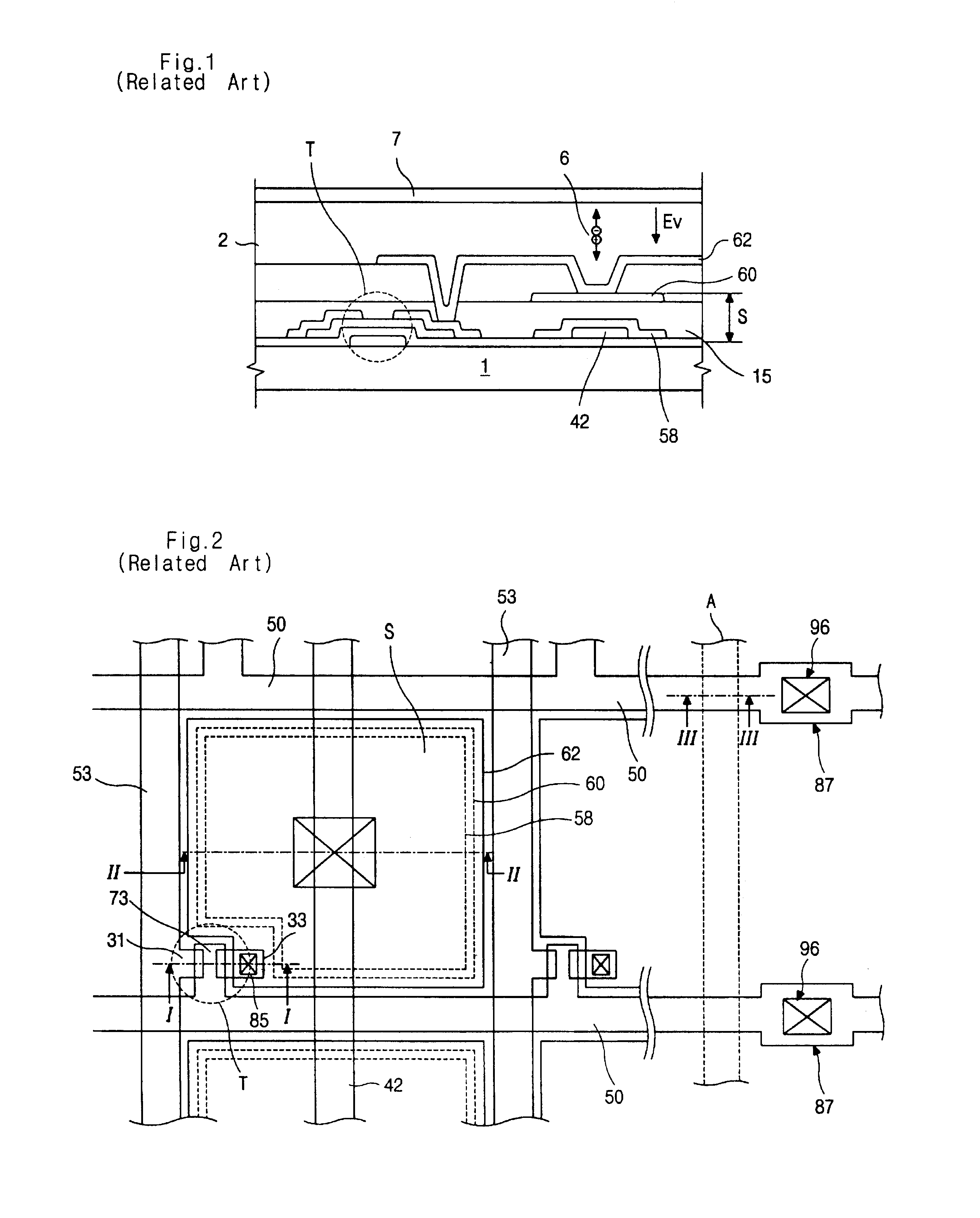
As described above, since the present invention employs the etching stopper on the first insulation layer, the etching ratio of the protection layer and the second insulation layer, which are stacked over the drain electrode and over the capacitor electrode, is controlled. Thus, over-etch caused by a difference in the number of etching layers is prevented. The EPD can also be employed.

second embodiment

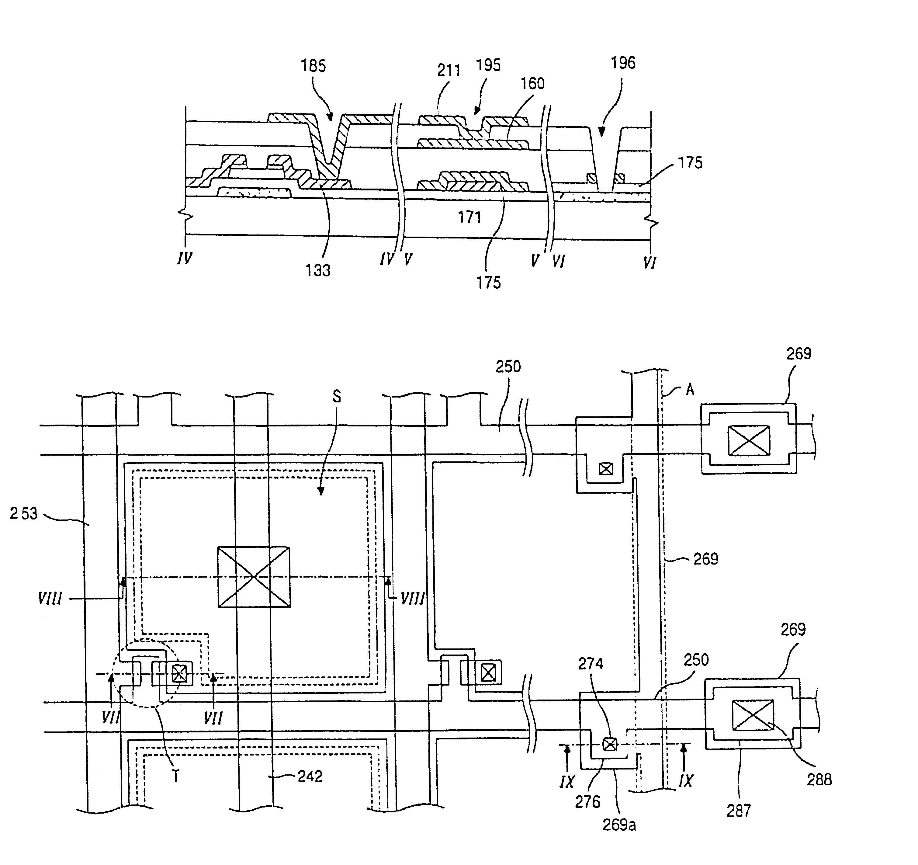
Moreover, since the gate line is electrically connected to the etching stopper through the gate line contact hole in the second embodiment, gate line open-circuits caused by static electricity during a dry etching process are prevented. Therefore, the manufacturing yield is raised, and the manufacturing defect caused in the array substrate is decreased. The EPD can also be employed.


PUM


Abstract

An array substrate for use in an X-ray sensing device is fabricated using an etching stopper that enables good control of the etching process and that prevents over-etch of drain electrodes and second capacitor electrodes while forming contact holes and a cutting furrow. The etching stopper is located in a tiling portion that is utilized for tiling substrates to form a large-sized X-ray detector. During fabrication, gate lines can have gate-protruded portions located near the etching stopper, and the etching stopper can have stopper-protruded portions near the gate lines. The stopper-protruded portions electrically connect to the gate-protruded portions through gate line contact holes such that the etching stopper and the gate lines have equipotentials. This can reduce static electricity damage.

Description

This application claims the benefit of Korean Patent Application No. 1999-67850, filed on Dec. 31, 1999, which is hereby incorporated by reference for all purposes as if fully set forth herein.1. Field of the InventionThe present invention relates to X-ray detectors. More particularly, it relates to Thin Film Transistor (TFT) array substrates for use in X-ray detectors.2. Description of Related ArtA widely used method of medical diagnosis is the X-ray film. As such films produce photographic images, time consuming film-processing procedures are required to obtain the results. However, digital X-ray sensing devices (referred to hereinafter as X-ray detectors) that employing thin film transistors have been recently developed. Such X-ray sensing devices have the advantage of providing real time diagnosis.FIG. 1 is a cross-sectional view illustrating one pixel of an array substrate of a conventional X-ray sensing device. That X-ray sensing device includes a Thin Film Transistor (TFT) "T...

Claims


Application Information

Patent Timeline
Patent Type & Authority Patents(United States)
IPC IPC(8): H01L21/00H01L21/302H01L29/786H01L29/66H01L21/02H01L21/461H01L31/00H01L21/20H01L21/31H01L21/44H01L21/469H01L27/146
CPCH01L27/14658H01L27/14687H01L27/14689H01L29/786
Inventor KWON, KEUK-SANG
Owner LG DISPLAY CO LTD
Why Eureka
Try Eureka