Integral capacitance for printed circuit board using dielectric nanopowders

a technology of integrated capacitance and printed circuit board, which is applied in the association of printed capacitors, printed circuit non-printed electric components, adhesive processes with surface pretreatment, etc., can solve the problems of major obstacles to microvia formation, the dielectric layer is unable to withstand substantial voltage, and the dielectric layer is unable to form vias

Inactive Publication Date: 2003-09-09
TPL INC
View PDF51 Cites 67 Cited by
  • Summary
  • Abstract
  • Description
  • Claims
  • Application Information

AI Technical Summary

Problems solved by technology

However, using pre-fired and ground ceramic nanopowders in the dielectric layer poses obstacles for the formation of vias (holes permitting electronic communication between layers of a laminated PCB).
The distribution within the dielectric layer of particles of different size often presents major obstacles to microvia formation, due to the presence of the larger particles.
Another problem associated with pre-fired ceramic nanopowders is the ability for the dielectric layer to withstand substantial voltage without breakdown occurring across the layer.
Although the pre-fired and ground dielectric formulations produced by solid phase reactions are acceptable for many electrical applications, they suffer from several disadvantages.
First, the milling step serves as a source of contaminants, which can adversely affect electrical properties.
Consequently, films produced using these powders are limited to thicknesses greater than the size of the largest particle.
Thirdly, powder suspensions or composites produced using pre-fired ground ceramic powders must be used immediately after dispersion, due to the high sedimentation rates associated with large particles.

Method used


Image

  • Integral capacitance for printed circuit board using dielectric nanopowders
  • Integral capacitance for printed circuit board using dielectric nanopowders
  • Integral capacitance for printed circuit board using dielectric nanopowders

Examples


first embodiment

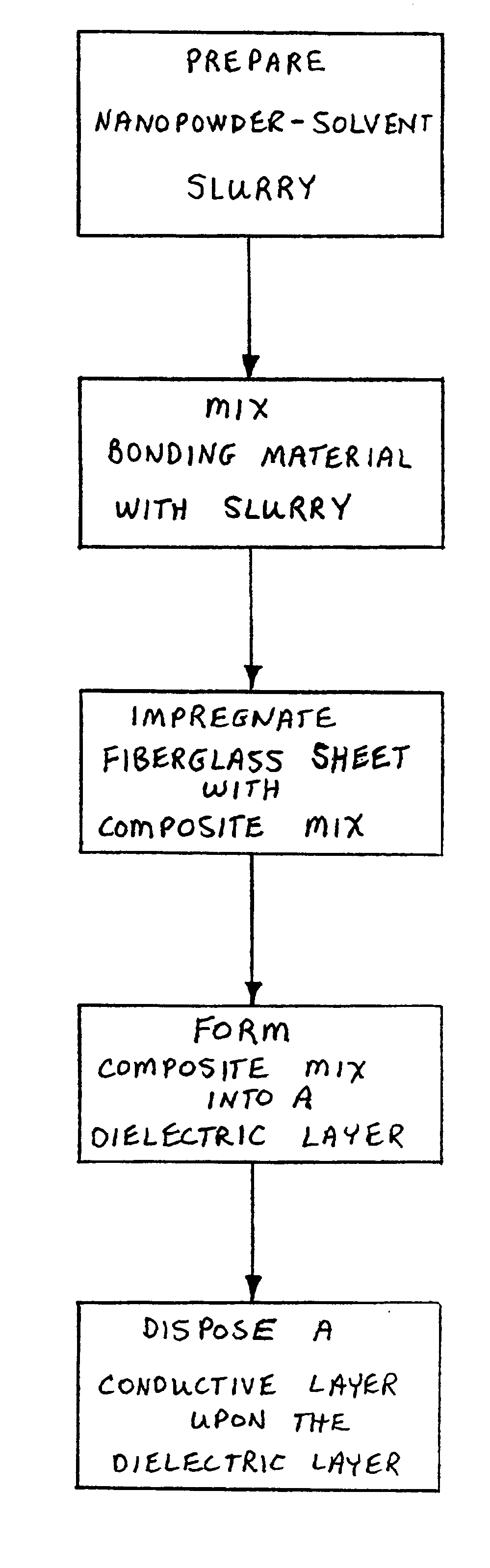
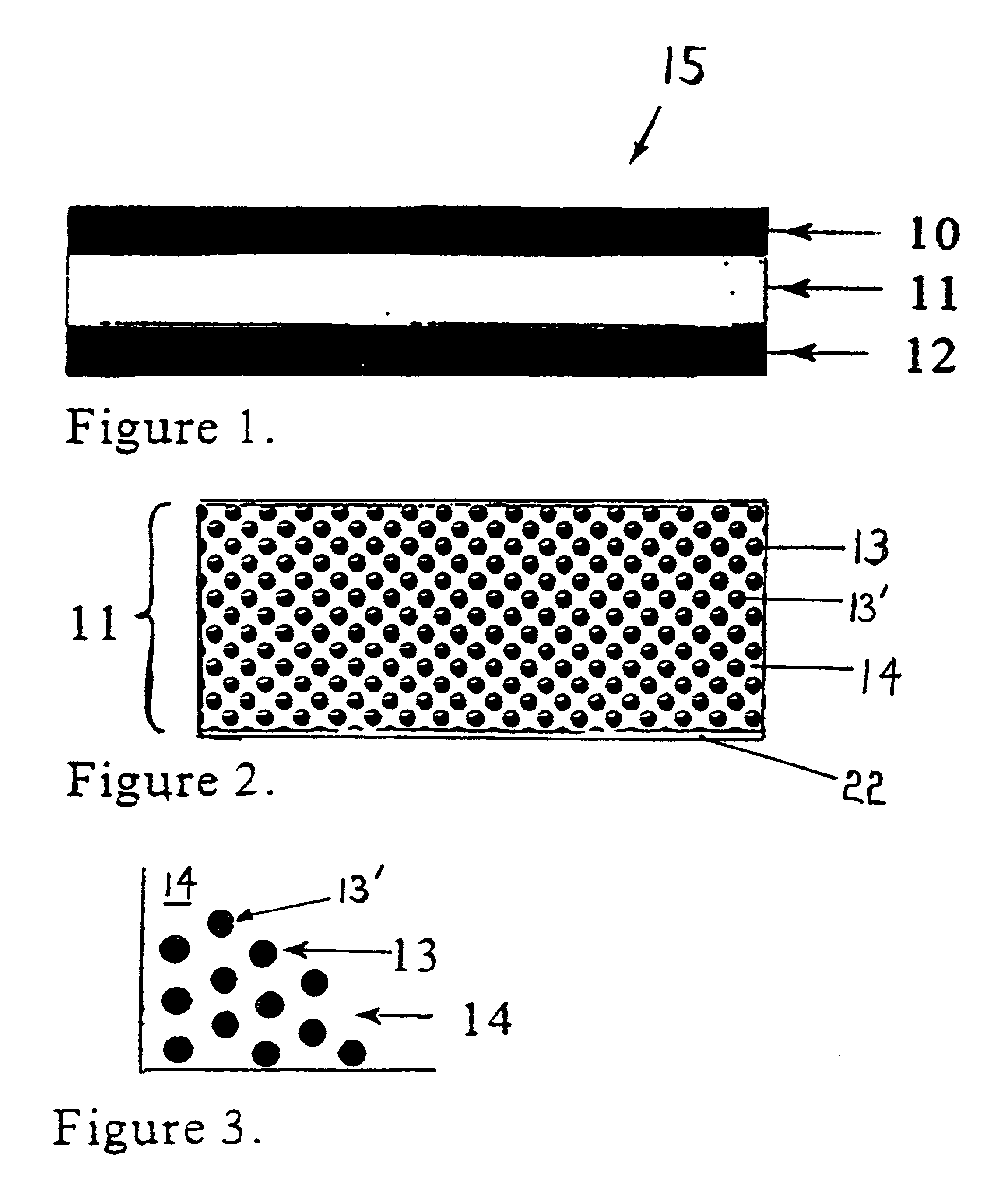
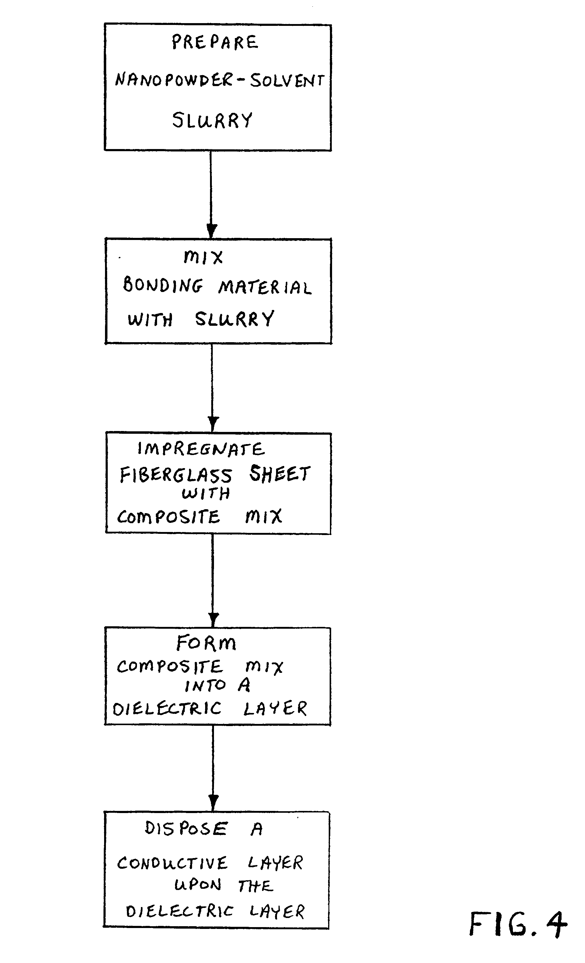
In this first embodiment of the invention, the composite-impregnated fiberglass sheet comprises the dielectric layer 11. Subsequent to the production of the dielectric layer 11 as described above, the conductive layers 10 and 12 are disposed upon one, or usually two sides, of the dielectric layer. This may be done in a lamination press, wherein the conductive layers 10, 12 (e.g. thin copper sheets, each about 1 or 2 mils thick) are pressed against the dielectric layer 11, and the entire sandwiched assembly heated to cause the polymer matrix in the dialectic layer 11 to bond to the conductive sheets. Accordingly, in many applications of the invention, it is desirable to employ a polymer with a relatively low glass transition temperature so that conventional lamination presses can induce the bonding between layer 11 and the conduction sheets 10, 12. Besides the foregoing lamination manner of disposing the conductive layers upon the dielectric layer, alternative modes such as attachmen...

second embodiment

In the invention, an integral capacitor is created by coating a conductive foil or sheet 12 with a composite mixture which includes a bonding matrix material, solvent, and hydrothermally prepared nanopowders. The preparation of the composite mixture is generally the same as previously described, that is, a nanopowder is suspended in a solvent to create a suspension slurry, and the bonding material, usually a polymer, is mixed with the slurry. Coating of a conductive foil substrate 12 such as copper is performed by physical placement of the composite mixture on the foil and subsequent removal of the solvent. For example, the uncured composite mixture may be extruded onto a conductive layer 12, and then the composite and conductive layer placed into a curing oven for about 10 minutes at about 180.degree. F. In this embodiment, no fiberglass sheet is included in the dielectric layer, rather the composite mixture is by itself cured to form the dielectric layer 11. The dielectric layer 1...


PUM

PropertyMeasurementUnit
particle sizeaaaaaaaaaa
dielectric constantaaaaaaaaaa

Abstract

A method for producing integral capacitance components for inclusion within printed circuit boards. Hydrothermally prepared nanopowders permit the fabrication of a very thin dielectric layers that offer increased dielectric constants and are readily penetrated by microvias. Disclosed is a method of preparing a slurry or suspension of a hydrothermally prepared nanopowder and solvent. A suitable bonding material, such as a polymer is mixed with the nanopowder slurry, to generate a composite mixture which is formed into a dielectric layer. The dielectric layer may be placed upon a conductive layer prior to curing, or conductive layers may be applied upon a cured dielectric layer, either by lamination or by metallization processes, such as vapor deposition or sputtering.

Description

1. Field of the Invention (Technical Field)The present invention relates to providing capacitance in printed circuit boards, more specifically to a method and apparatus for providing a layer or layers of integral capacitance in printed circuit boards using dielectric nanopowders.2. Background ArtPrinted circuit boards (PCBs) typically are constructed in a laminated form. Several layers of laminate are used in a board for providing electrical connections to and among various devices located on the surface of the board. These surface devices consist of integrated circuits and discrete passive devices, such as capacitors, resistors and inductors, and the like. The discrete passive devices occupy a high percentage of the surface area of the complete PCB. Therefore, in order to increase the available surface of the PCBs, there have been a variety of past efforts to locate passive devices, including capacitors, in a embedded, or subsurface, configuration within the board. When passive dev...

Claims


Application Information

Patent Timeline
Patent Type & Authority Patents(United States)
IPC IPC(8): H05K1/16
CPCH05K1/162H05K3/4688H05K2201/0209H05K2201/0257H05K2201/0317H05K2201/09309
Inventor HARTMAN, WILLIAM F.SLENES, KIRK M.LAW, KRISTEN J.
Owner TPL INC
Why Eureka
Try Eureka