
Tape carrier having high flexibility with high density wiring patterns

Inactive Publication Date: 2003-10-14
VISTA PEAK VENTURES LLC
View PDF19 Cites 15 Cited by
  • Summary
  • Abstract
  • Description
  • Claims
  • Application Information

AI Technical Summary

Problems solved by technology

Therefore, process steps for manufacturing such a tape carrier become complicated, and throughput of manufacturing is also deteriorated.
Thus, it needs many kinds of materials used for fabricating such tape carrier, and it results in increase of the cost.
Therefore, when the tape carrier is bent or a stress is applied to the tape carrier from the outside, the stress is concentrated at portions near end portions of the slit shaped openings so that there is a possibility that the base film is damaged.
However, when the thickness of the base film is increased, it becomes difficult to bend the tape carrier, and it results in increase of weight and the cost of the tape carrier.
However, in this structure, since the round openings are formed between adjacent wiring patterns, when respective spaces between adjacent wiring patterns are small, it is difficult to form appropriately the round openings in the base film such that sufficient flexibility of the base film is obtained.
Therefore, it is not appropriate to use this structure when spaces between wiring patterns are small.
Thus, this structure does not suit such recent tape carrier in which wiring patterns are formed in high density.
Also, in this structure, since small round openings are formed between respective wiring patterns, it is impossible to enlarge the proportion of areas of openings in the bending area of the tape carrier sufficiently.
Therefore, it is impossible to obtain good bending characteristics, such as sufficient flexibility at desired portion or portions of a tape carrier.

Method used


Image

  • Tape carrier having high flexibility with high density wiring patterns
  • Tape carrier having high flexibility with high density wiring patterns
  • Tape carrier having high flexibility with high density wiring patterns

Examples


Embodiment Construction

With reference to the drawings, an embodiment of the present invention will now be explained in detail.

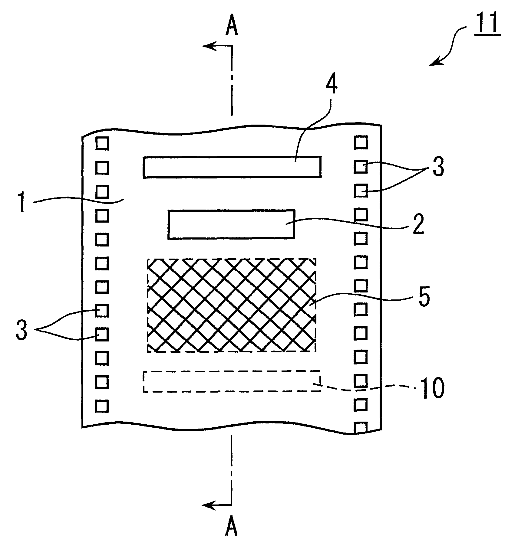
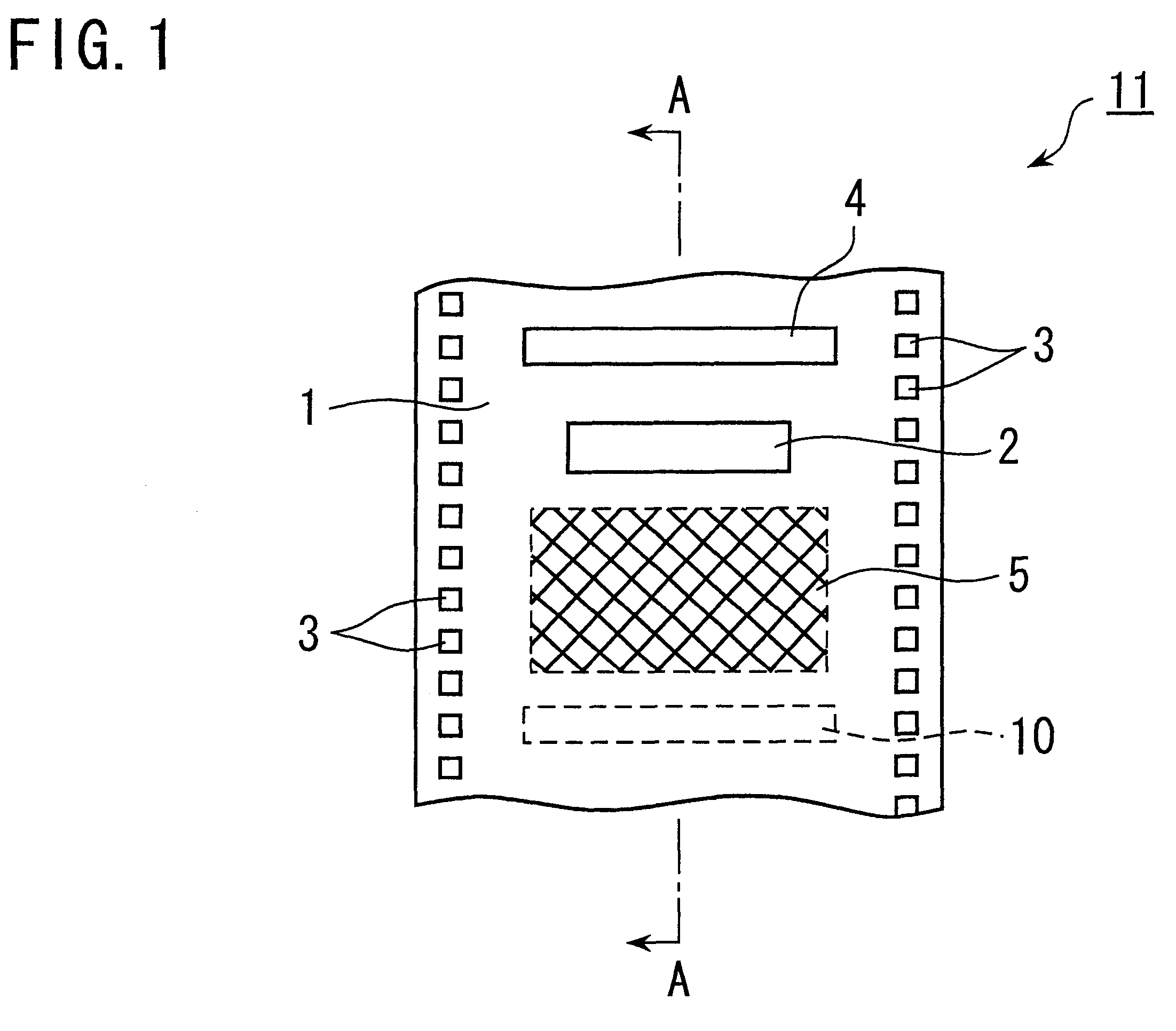
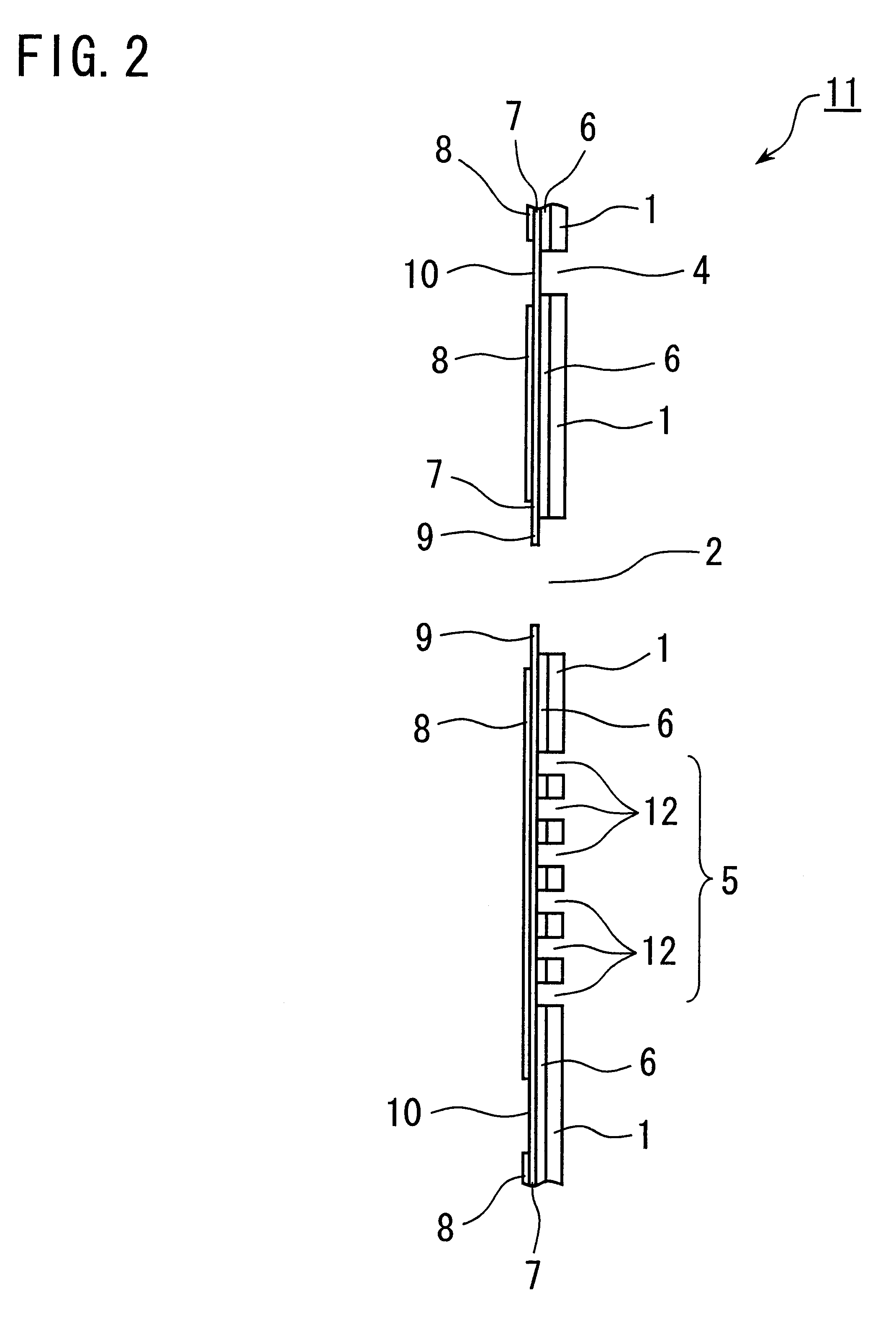
FIG. 1 is a plan view schematically showing a tape carrier according to an embodiment of the present invention. FIG. 2 is a schematic cross sectional view taken on line A--A of FIG. 1.

The tape carrier according to the present invention is a tape carrier for constituting, for example, a tape carrier package (TCP). The TCP is used, for example, in a liquid crystal display and the like.

The tape carrier shown in FIG. 1 and FIG. 2 comprises an insulating base film 1 having a tape like shape. The base film 1 is fabricated from a polymer or resin film having high flexibility, for example, a polyimide film having a thickness of 75 .mu.m (micrometers) such as UPILEX-S.RTM. (Poly [1,1',3,3'-tetrahydro-1,1',3,3'-tetraoxo[5,5'-bi-2H-isoindole]-2,2'-diyl)-1,4-phenylene]) manufactured by UBE INDUSTRIES, LTD.

On one surface of the base film 1, there are formed wiring patterns 7 via an adhesive lay...


PUM


Abstract

A tape carrier with high density wiring patterns and having high flexibility, a tape carrier package using such tape carrier, and a method of manufacturing them. The tape carrier has a base film made of an insulating material and having wiring patterns formed thereon. The tape carrier also has a bending area for bending the tape carrier therein. In the bending hole region, a plurality of round holes are formed regularly. Diameter of each of the holes is larger than a space between the wiring patterns in the bending area. Preferably, the centers of the holes are located at grid points of an assumed predetermined grid and at the intersections of diagonal lines connecting the grid points. Also, the center of each of the plurality of holes is located on the center line of a space between adjacent wiring patterns in the bending area.< / PTEXT>

Description

1. Field of the InventionThe present invention relates generally to a tape carrier in which wiring patterns are formed on an insulating base film, and a method of manufacturing such a tape carrier. More particularly, the present invention relates to a tapes carrier with high density wiring patterns which is bent easily and which has a high reliability, and a method of manufacturing such a tape carrier. The present invention also relates to a tape carrier package (TCP) which is fabricated by attaching a semiconductor chip on such tape carrier, and a liquid crystal display device having such a TCP.2. Description of the Related ArtA tape carrier package (TCP) used in a liquid crystal display and the like is often used in condition it is bent or folded at predetermined portion or portions thereof. Conventionally, TCP's having various structures are used to obtain good bending characteristics such as easiness of bending and the like.For example, there is known a tape carrier structure di...

Claims


Application Information

Patent Timeline
IPC IPC(8): H05K1/00H05K3/28H01L21/60G02F1/1345
CPCH05K1/028H01L24/50H05K3/28H05K2201/10681H05K2201/0394H01L2224/50H01L2924/00012G02F1/13
Inventor ATOU, NORIAKI
Owner VISTA PEAK VENTURES LLC
Learn More