Array-built-in-self-test (ABIST) for efficient, fast, bitmapping of large embedded arrays in manufacturing test

Inactive Publication Date: 2003-11-04
GOOGLE LLC
View PDF16 Cites 85 Cited by
  • Summary
  • Abstract
  • Description
  • Claims
  • Application Information

AI Technical Summary

Problems solved by technology

Testing of these embedded memories is therefore complicated because any access to these memories during normal operation of the chip is mediated by the associated logic.
In many cases, the cost of testing the device is comparable to the cost of manufacturing the raw die in the fabrication plant.
The cost of testing is approximately proportional to the product of the test time and the cost of the testing equipment.
A drawback to this approach is that the extra bus lines and pads increase the size of the semiconductor die and the extra pads increase the number of pins required of the tester.
Since the trend is toward wide memories of increasingly large capacity in modern ICs, the number of e

Method used


Image

  • Array-built-in-self-test (ABIST) for efficient, fast, bitmapping of large embedded arrays in manufacturing test
  • Array-built-in-self-test (ABIST) for efficient, fast, bitmapping of large embedded arrays in manufacturing test
  • Array-built-in-self-test (ABIST) for efficient, fast, bitmapping of large embedded arrays in manufacturing test

Examples


Embodiment Construction

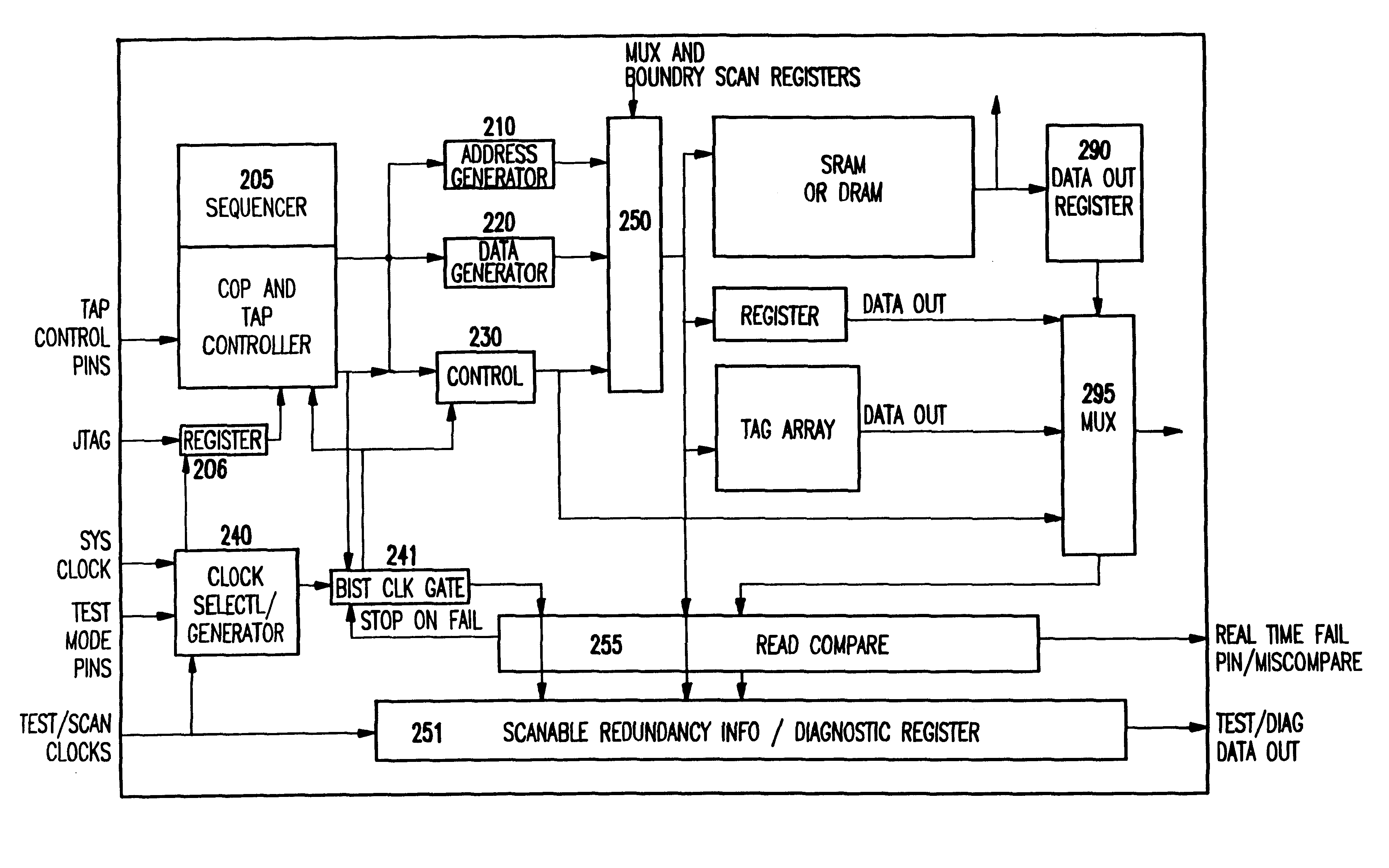
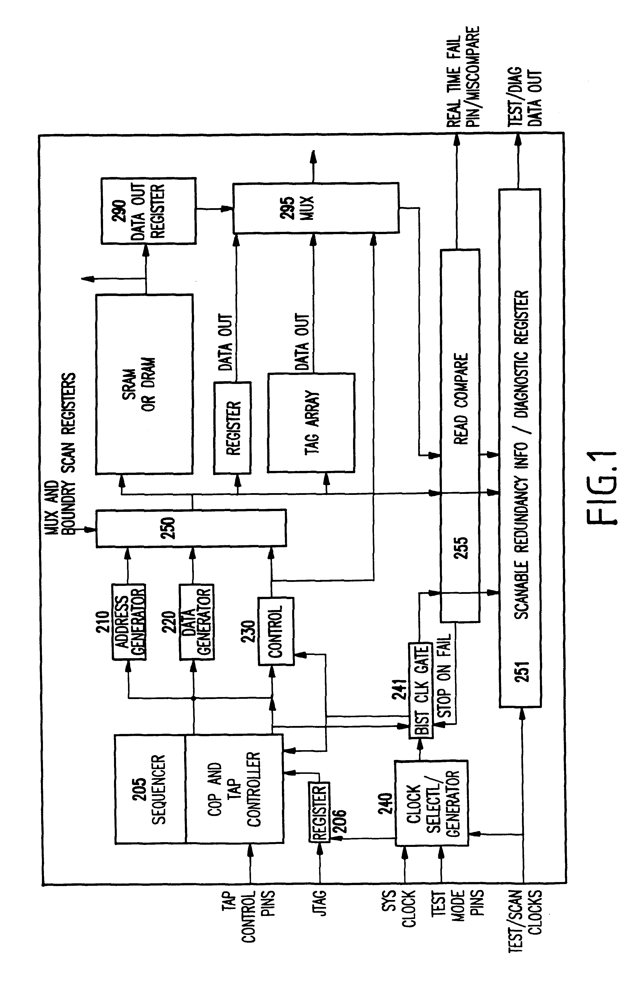
The present invention is preferably embodied in an integrated circuit chip having logic, DRAM or SRAM embedded in the logic, and a BIST macro for testing the DRAM or SRAM. The embedded DRAM or SRAM is integral to a chip having a logic function, such as a complex gate array or standard cell, a microprocessor, a Digital Signal Processor (DSP), or an Application Specific Integrated Circuit (ASIC). The present invention logic chip may include one or more such embedded DRAMs and / or SRAMS.

FIG. 1 is a logic block diagram of the BIST macro according to the present invention. The BIST block preferably includes a sequencer 205, an address generator 210, a data generator 220, a control block 230, a clock generator 240, a clock gate 241, a multiplexor to mux the address, data, and control to any embedded array 250, a read compare register 255 to compare the data read back from the arrays to the data written, a diagnostic register 251 to capture the compare output and failing address, and a Jtag...


PUM


Abstract

A structure and method for an integrated circuit which includes read/write memory having a plurality of memory devices, each of the memory devices having a unique address; a built-in self-test (BIST) engine, the BIST engine having a controller responsive to a test enable signal and operative to generate and store test data in the read/write memory; a comparator operative to compare retrieved data read from the read/write memory and the test data during a first pass test, the comparator identifying failed cycles where the retrieved data does not correspond correctly to the test data; and a diagnostic unit operative to store the failed cycles and being responsive to the controller generating and storing the test data in the read/write memory and operative to store failed data and failing addresses during a first pass test, wherein the BIST engine stops only at each of the failed cycles during the first pass test.

Description

1. Field of the InventionThe present invention relates to semiconductor integrated circuits and, more particularly, to test circuits built into the integrated circuits that enable efficient testing of embedded memory, especially read / write memory.2. Description of the Related ArtAs integrated circuits achieve higher and higher levels of integration it is common to find several memory blocks of differing sizes embedded within blocks of logic in the integrated circuit. A typical example of embedded memory is the data and instruction cache memories along with their associated tag and valid data cache memories that are embedded in most modem microprocessors. These memories are called "embedded" because they are not directly accessible from the input and output pins of the integrated circuit chip. Instead, an embedded memory is separated by logic blocks from the input and output pins in ordinary operation of the circuit. Testing of these embedded memories is therefore complicated because...

Claims


Application Information

Patent Timeline
IPC IPC(8): G11C29/04G11C29/44G11C29/00
CPCG11C29/44G11C2207/104G11C29/00
Inventor HEASLIP, JAY G.MAIER, GARY W.SALEM, GERARD M.VON REYN, TIMOTHY J.
Owner GOOGLE LLC
Why Eureka
Try Eureka