Method of forming a silicon nitride layer on a substrate

a technology of silicon nitride and substrate, which is applied in the direction of coating, chemical vapor deposition coating, metallic material coating process, etc., can solve the problems of high temperature deposition, outdiffusion of dopants, and high deposition rate of silicon nitride layer

Inactive Publication Date: 2003-11-11
APPLIED MATERIALS INC
View PDF7 Cites 61 Cited by
  • Summary
  • Abstract
  • Description
  • Claims
  • Application Information

AI Technical Summary

Problems solved by technology

Although higher temperatures result in a higher deposition rate of the silicon nitride layer on a wafer, high temperature deposition has its disadvantages.
One disadvantage is that high temperature processing causes outdiffusion of dopants from, for example, P-type conductivity or N-type conductivity regions (P- or N-doped regions) of a semiconductor wafer.

Method used


Image

  • Method of forming a silicon nitride layer on a substrate
  • Method of forming a silicon nitride layer on a substrate
  • Method of forming a silicon nitride layer on a substrate

Examples


Embodiment Construction

In the following description, for purposes of explanation, numerous specific details are set forth in order to provide a thorough understanding of the present invention. It will be evident, however, to one skilled in the art that the present invention may be practiced without these specific details. In certain instances specific apparatus, structures, and methods have not been described so as not to obscure the present invention.

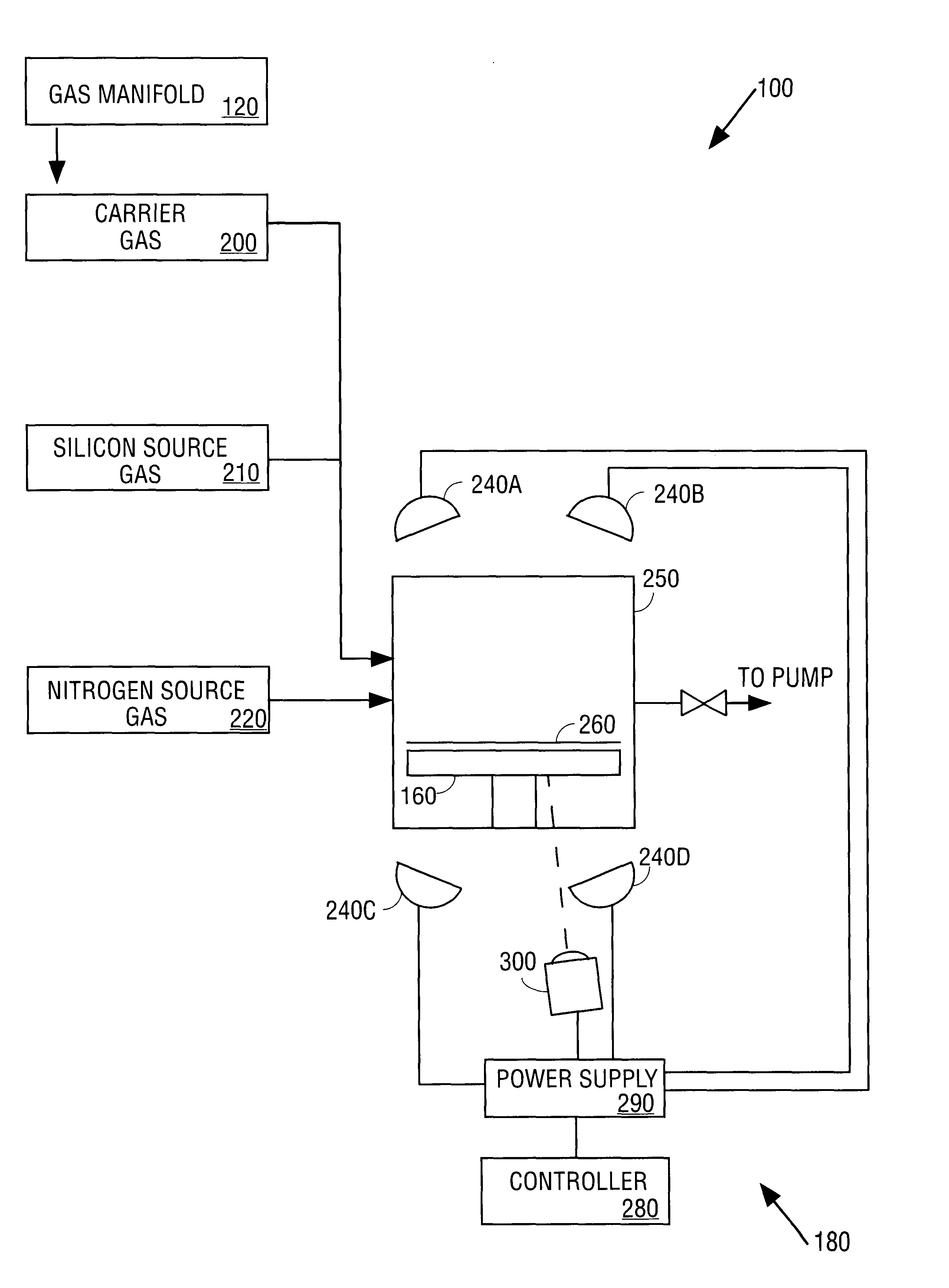
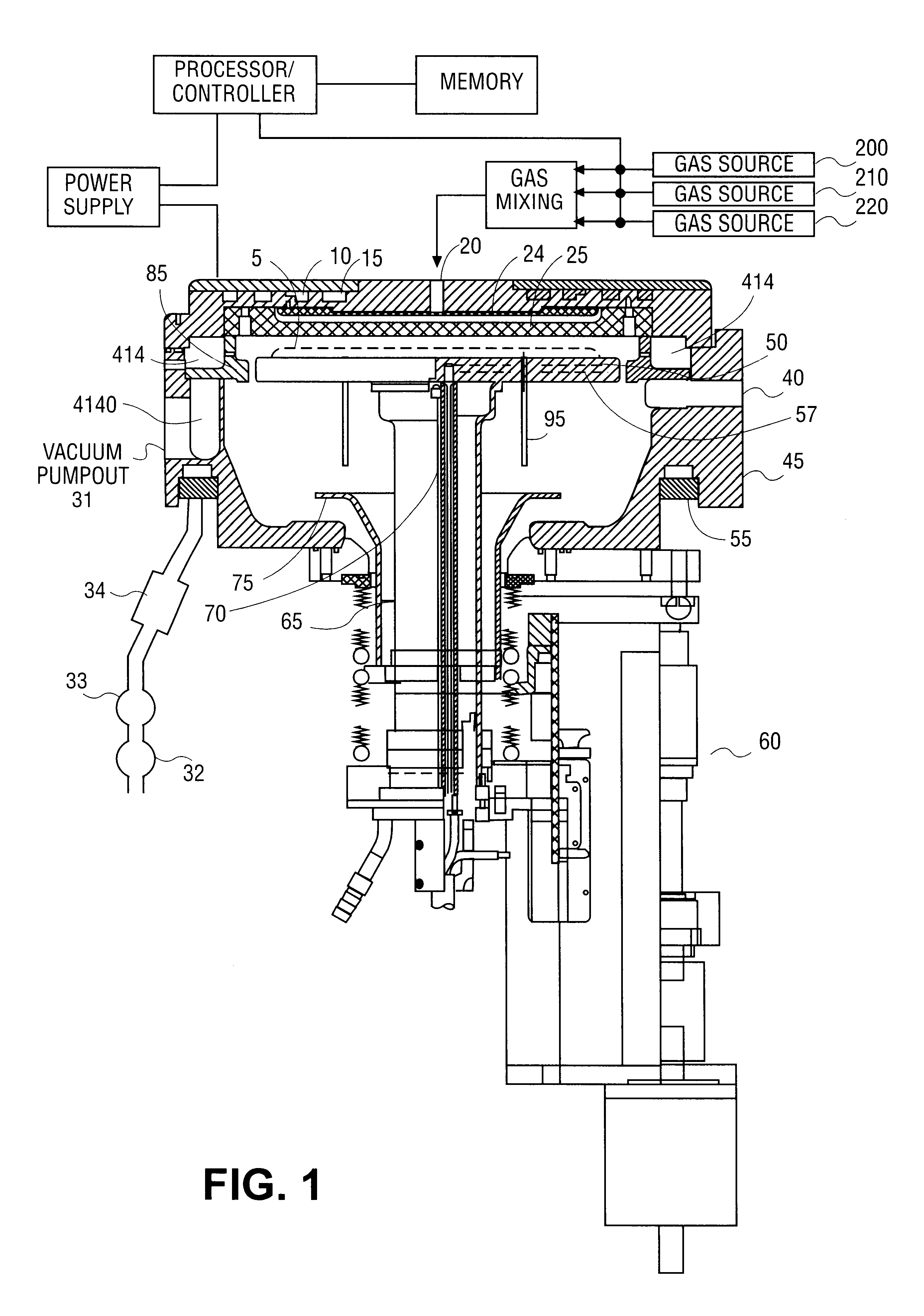
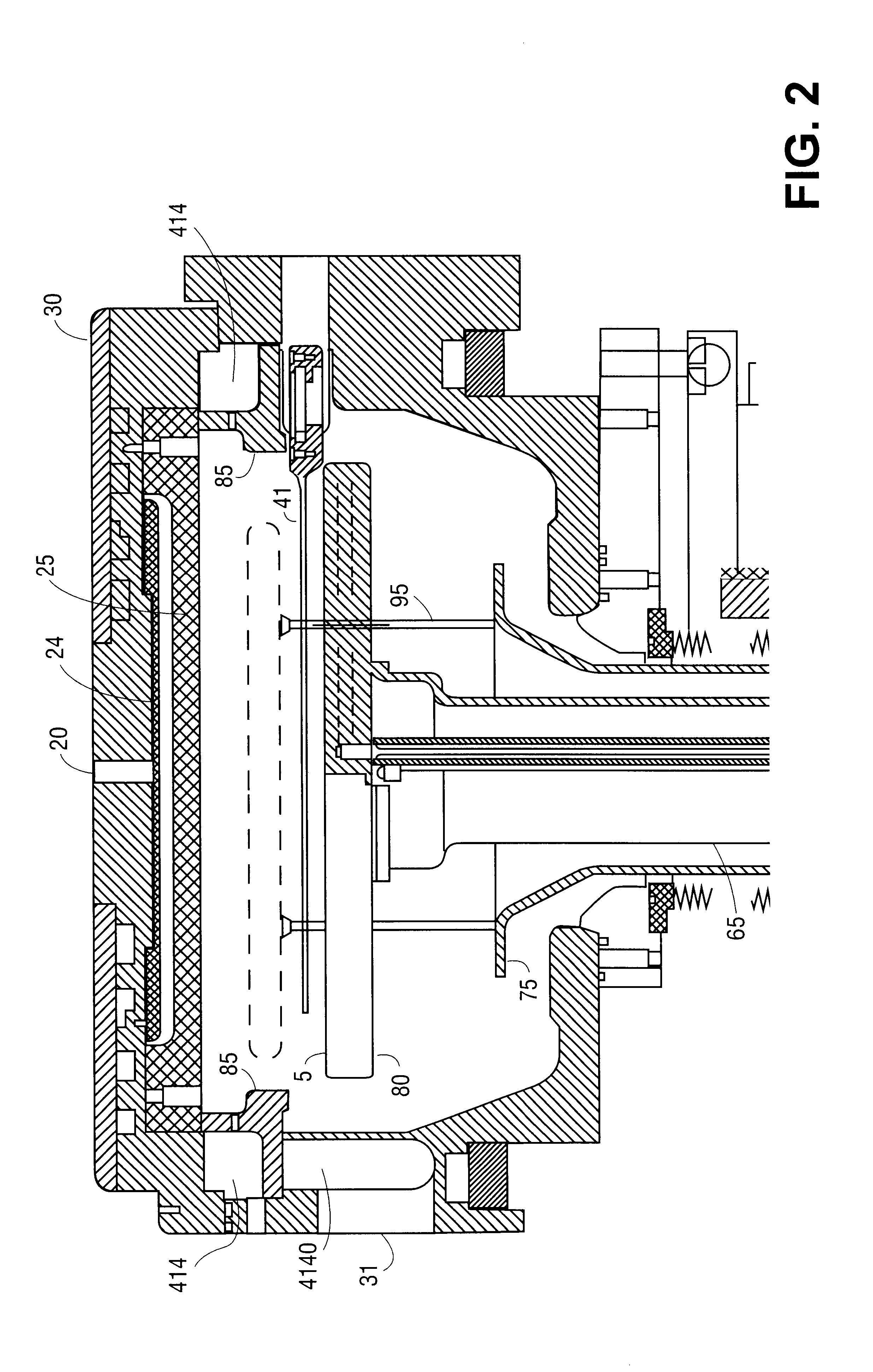
The invention relates to methods and apparatuses of forming a silicon nitride film layer on a substrate such as a semiconductor wafer. In one embodiment, the film or layer is formed on a semiconductor wafer that is located on a susceptor within a single wafer processing chamber that is heated by using radiant or resistive heat. A mixture of gases, including a nitrogen source gas, a silicon source gas, and a carrier gas, are introduced into the chamber to form the Si.sub.3 N.sub.4 film or layer. The wafer is exposed to the mixture at a wafer temperature of be...


PUM

PropertyMeasurementUnit
temperatureaaaaaaaaaa
pressureaaaaaaaaaa
partial pressureaaaaaaaaaa

Abstract

The invention provides methods and apparatuses of forming a silicon nitride layer on a semiconductor wafer. A semiconductor wafer is located on a susceptor within a semiconductor processing chamber. A carrier gas, a nitrogen source gas, and a silicon source gas are introduced into the semiconductor processing chamber and a semiconductor wafer is exposed to the mixture of gases at a pressure in the chamber in the range of approximately 100 to 500 Torr.

Description

1. Field of the InventionThis invention relates generally to deposition technologies in integrated circuit chip processing and more particularly to the deposition of silicon nitride films.2. Discussion of Related ArtThe manufacture of semiconductor integrated circuits generally involves the formation of a plurality of layers of material on a semiconductor (e.g., silicon) wafer, each layer serving specific functions generally related to the routing and isolating of specific signals. One or more of these layers may comprise silicon nitride (Si.sub.3 N.sub.4) as an insulator or mask. A conventional method of forming a silicon nitride layer on a wafer involves locating the wafer on a susceptor within a processing chamber and introducing a mixture of gases such as a silicon source gas, a nitrogen source gas, and a carrier gas into the processing chamber. The gases combine in the processing chamber at generally a pressure of about 300 millitorr (mTorr) to form the silicon nitride layer or...

Claims


Application Information

Patent Timeline
Patent Type & Authority Patents(United States)
IPC IPC(8): C23C16/34C23C16/44C23C16/42H01L21/31H01L21/318
CPCC23C16/4412C23C16/345H01L21/0217H01L21/02271H01L21/02211C23C16/45591
Inventor YANG, MICHAEL X.KAO, CHIEN-TEHLITTAU, KARLCHEN, STEVEN A.HO, HENRYYU, YING
Owner APPLIED MATERIALS INC
Why Eureka
Try Eureka