

System and method for a high speed, bi-directional, zero turnaround time, pseudo differential bus capable of supporting arbitrary number of drivers and receivers
a high-speed, bi-directional, zero-turnaround time technology, applied in the direction of logic circuits, pulse techniques, reliability increasing modifications, etc., can solve the problems of static power dissipation, high-speed bussing becomes very difficult, and increases the delay of data propagation across the bus
- Summary
- Abstract
- Description
- Claims
- Application Information
AI Technical Summary
Benefits of technology
Problems solved by technology
Method used
Image

Examples
Embodiment Construction
)
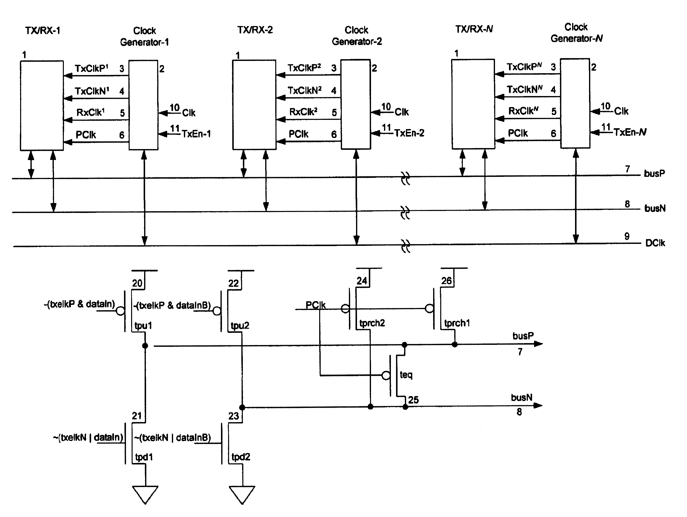
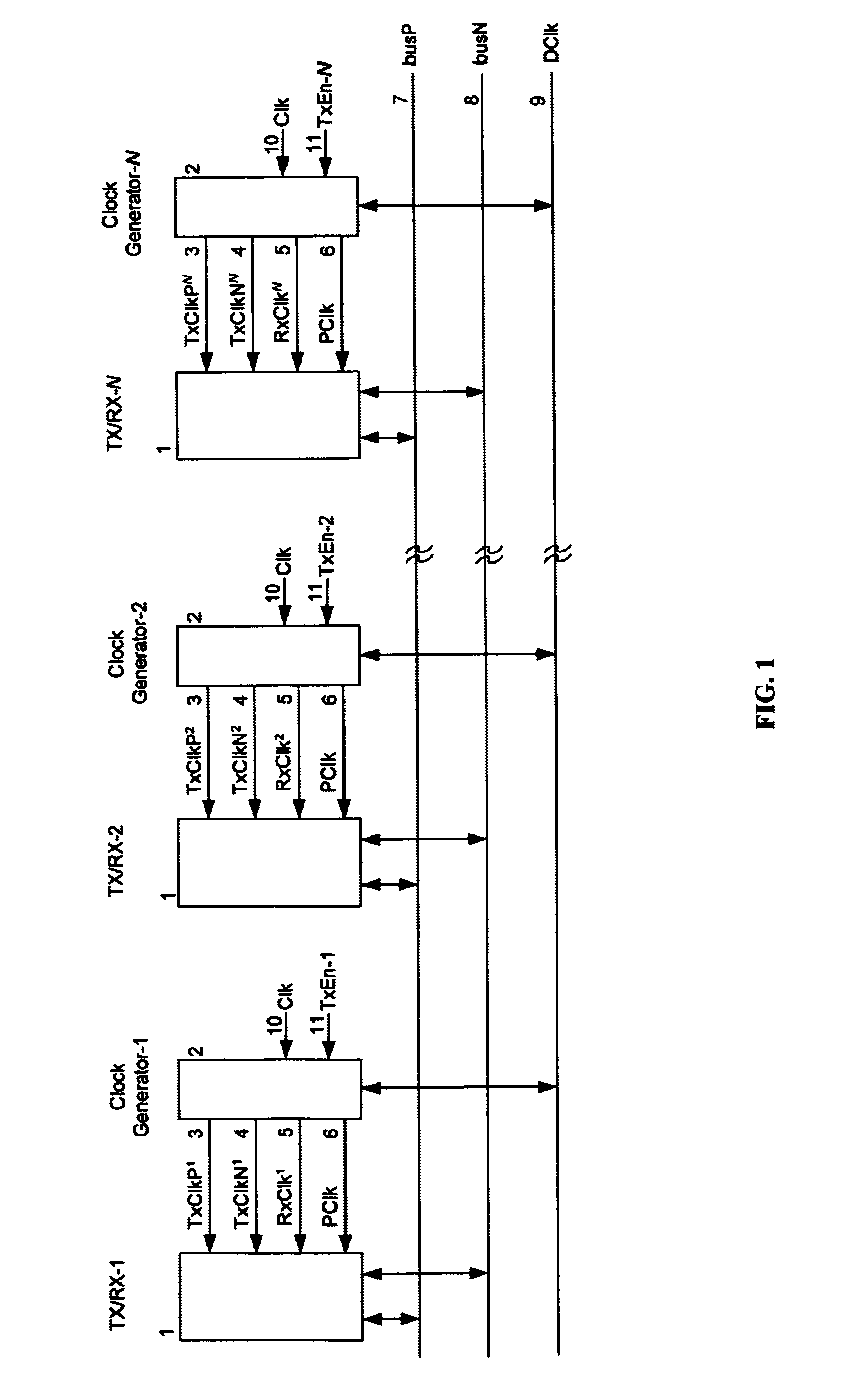
Bus Architecture
The invention here described is intended primarily for use in high-speed bussing for microprocessors and microelectronic devices.
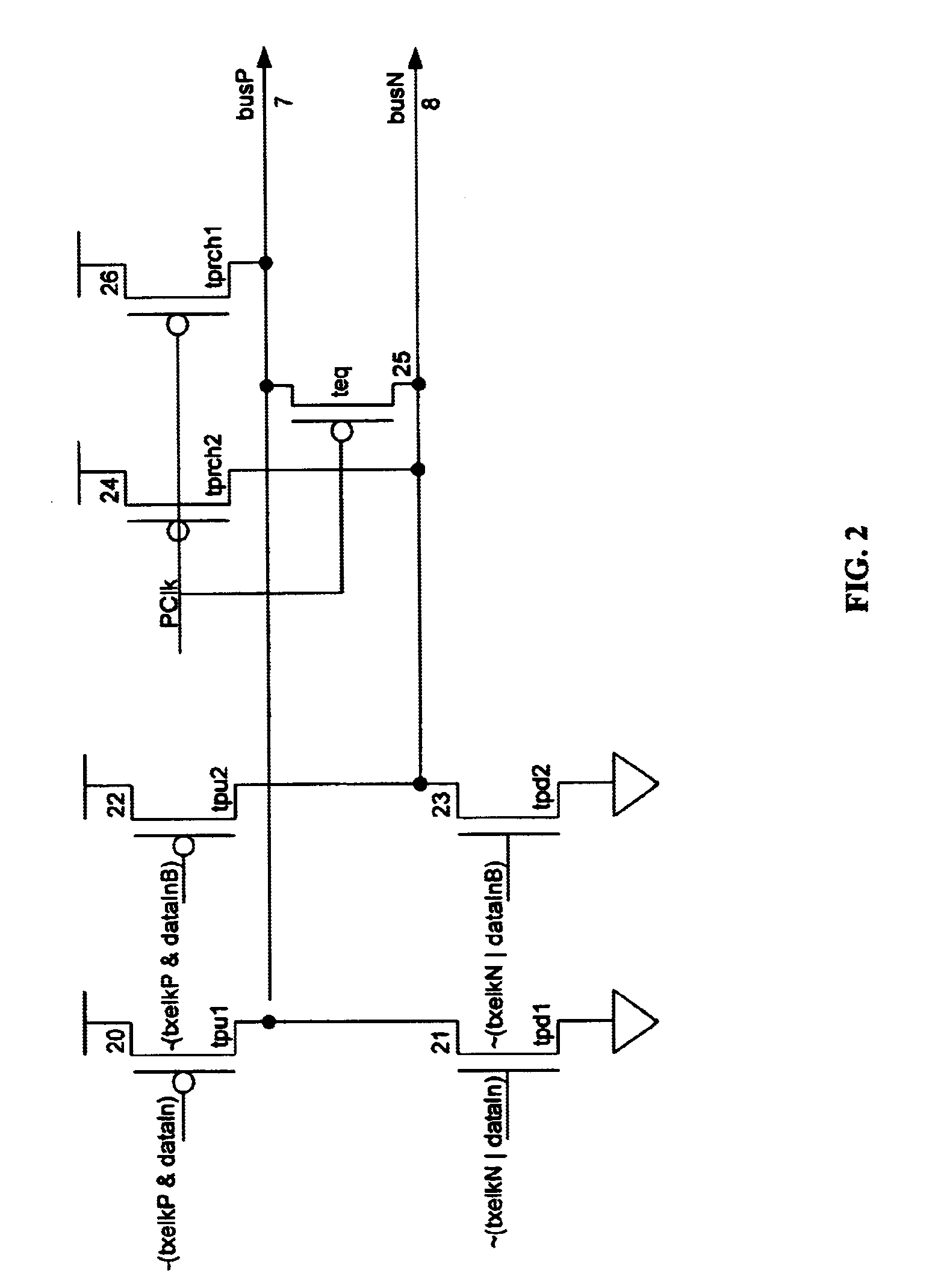
A typical differential bussing architecture contains two bus lines, the first bus line called the true bus and carrying the true data, and the second bus line called the complement bus and carrying the complement of the data. The present invention utilizes the differential bus lines in a uniquemanner to eliminate DC power dissipation and to reduce the pre-charge overhead by deploying a distributed pre-charge scheme in conjunction with a self-tracking signal which divides the clock cycle time into optimal pre-charge and evaluation phases. Therefore, the pre-charge scheme does not add to the latency of the data transfer on the bus.
FIG. 1 illustrates a block diagram of a pseudo differential bus scheme. Given a typical differential bus, with true bus lines, herein called busP 7, and complement bus lines, herein called busN 8, one embodiment of...
PUM
 Abstract
Description
Claims
Application Information