Bus interface circuit and receiver circuit

a receiver circuit and bus interface technology, applied in logic circuit coupling/interface arrangement, pulse technique, instruments, etc., can solve the problems of increasing access time and increasing power consumption, and achieve the effect of reducing the amplitude of the signal sent and reducing the time required

Inactive Publication Date: 2004-02-03
RENESAS ELECTRONICS CORP
View PDF3 Cites 14 Cited by
  • Summary
  • Abstract
  • Description
  • Claims
  • Application Information

AI Technical Summary

Benefits of technology

According to the present invention, the bus line is precharged to the precharge voltage, and the output circuit is configured such that a signal whose amplitude is determined by the precharge voltage and the fixed voltage is output to the bus line. This configuration reduces the amplitude of the signal sent to the bus line and reduces the time required by the output circuit and the receiver circuit to access the bus.

Problems solved by technology

This delay time results in an increase in access time and becomes one of the limiting factors of the high-speed operation of the memory system.
On the other hand, an increase in current drive capability of the output buffer circuit in an attempt to speed up a transition time of a signal at the far-end of the bus line would lead to an increase in power consumption.

Method used


Image

  • Bus interface circuit and receiver circuit
  • Bus interface circuit and receiver circuit
  • Bus interface circuit and receiver circuit

Examples


Embodiment Construction

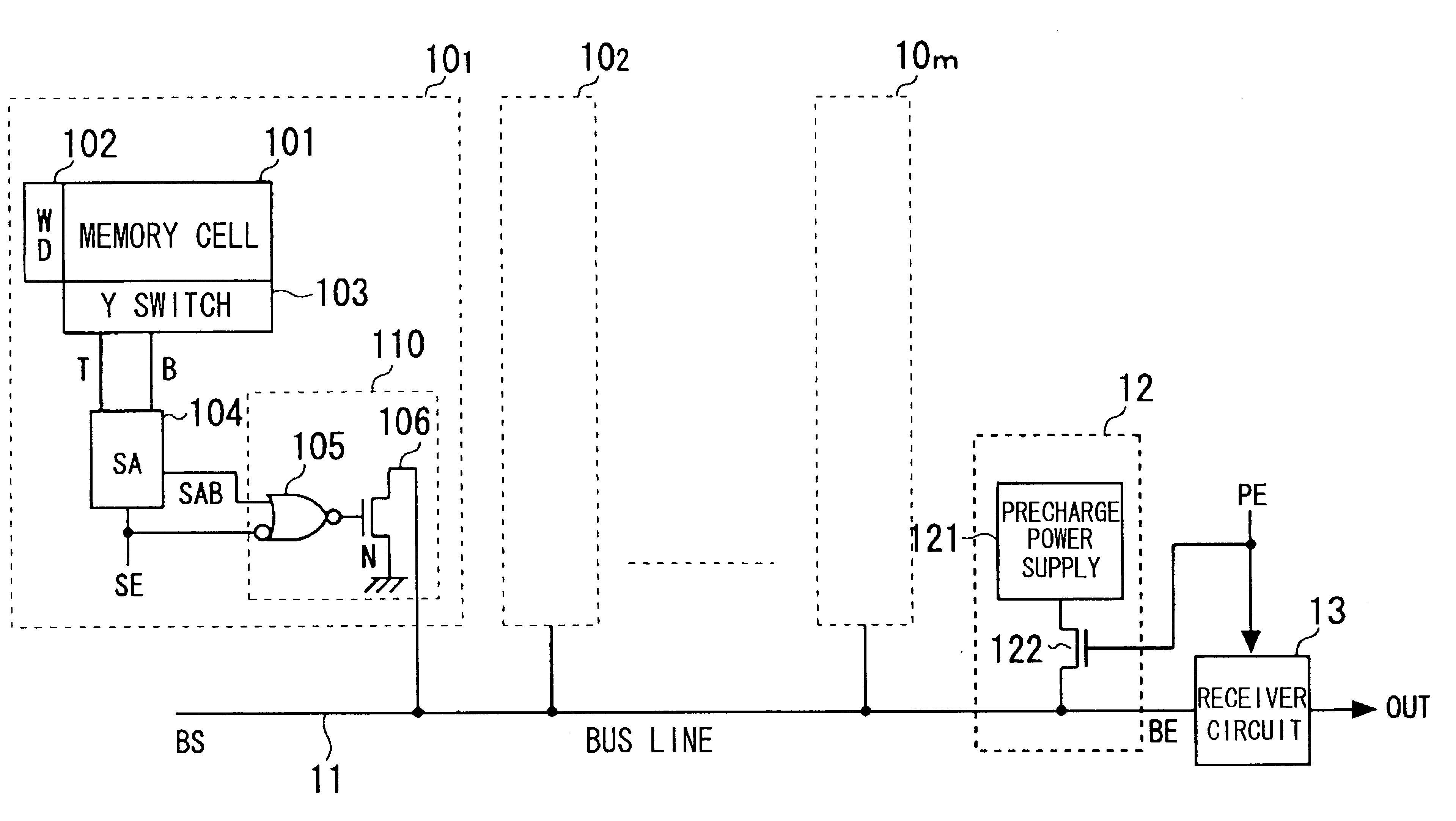
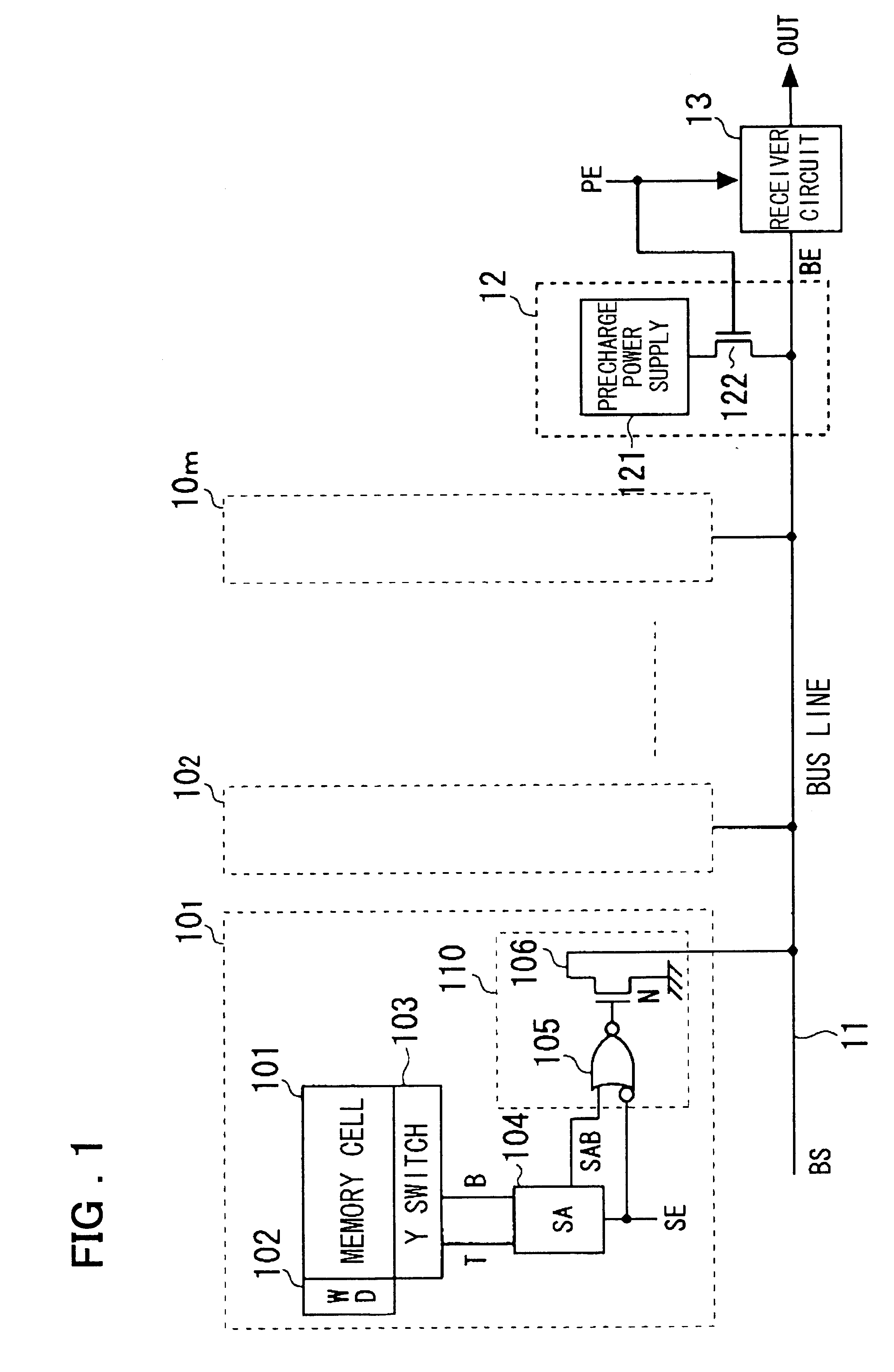
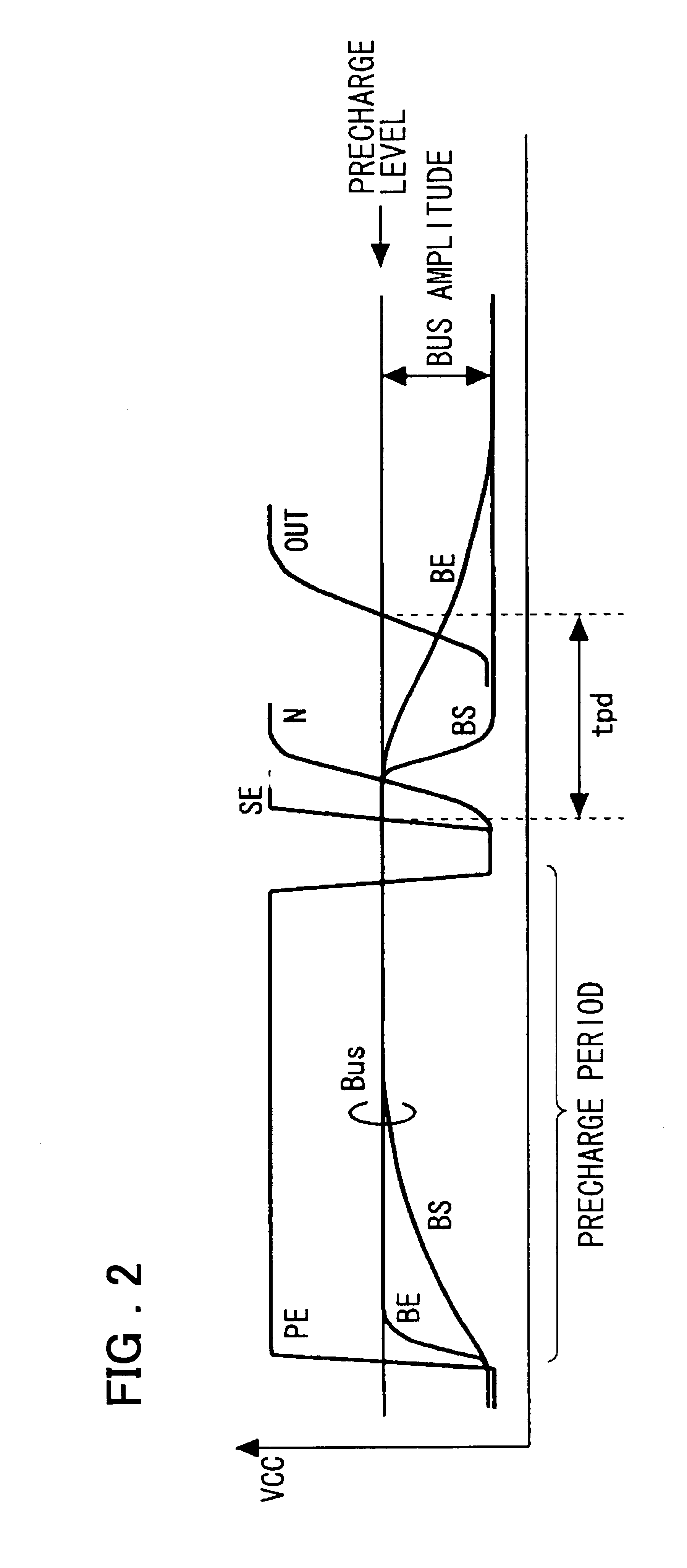
Preferred embodiments of the present invention will be described. One embodiment of a bus interface circuit according to the present invention comprises a precharge circuit (12 in FIG. 1) that precharges a bus line (11 in FIG. 1) with a precharge voltage that is a predetermined voltage (also termed "intermediate voltage") between the high-potential power supply voltage (VDD) and the low-potential power supply voltage (VSS). The precharge circuit (12) comprises a switch element (122 in FIG. 1) that is turned on or off based on a precharge control signal (PE) controlling the precharge operation. The precharge circuit (12) precharges the bus line (11) for a predetermined period (termed "precharge period") before an output circuit (for example, 110 in FIG. 1) driving the bus line (11) starts the output operation, and stops the precharge operation when the output circuit (110) outputs the output signal to the bus line (11).

The output circuit (110), which outputs data to the bus line (11)...


PUM


Abstract

A bus interface circuit includes a precharge circuit including a switch element which is inserted between a bus line and a precharge power supply, receives a precharge control signal PE at its control terminal, and is turned on when the precharge control signal is active. The precharge circuit precharges the bus line to a predetermined precharge voltage from the precharge power supply via the switch element that is turned on. The precharge voltage is a predetermined voltage between a high-potential power supply voltage VDD and a low-potential power supply voltage VSS. When a signal received by an output circuit for output to the bus line has a first logic value, an output circuit sets the bus line, which has been precharged to the precharge voltage, from the precharge voltage to the predetermined VSS.

Description

The present invention relates to a bus interface, and more particularly to a bus interface comprising an output circuit that drives a bus line, a precharge circuit that pre-charges the bus line, and a receiver circuit that receives a signal output to the bus line.A conventional bus control system for use in a memory device will be described. FIG. 8 is a diagram schematically showing an example of a conventional system configuration of a memory device. Referring to FIG. 8, a plurality of memory cell sub-array blocks 200.sub.l -200.sub.m are connected to a common bus line 210 to which a receiver circuit 220 is connected. The receiver circuit 220 receives data read from the sub-array blocks 200.sub.l -200.sub.m and outputs the received data.The sub-array blocks 200.sub.l -200.sub.m each have the same configuration, with the configuration of the sub-array block 200.sub.l shown in the figure. The sub-array block 200.sub.l comprises a memory cell array 201 in which a plurality of word lin...

Claims


Application Information

Patent Timeline
Patent Type & Authority Patents(United States)
IPC IPC(8): G11C7/10G11C11/417G06F3/00G06F13/00G11C11/41H03K19/0175
CPCG11C7/1057G11C7/1051G06F13/00
Inventor TAKAHASHI, HIROYUKIMATSUI, YUUJISATAKE, HIROYUKI
Owner RENESAS ELECTRONICS CORP
Why Eureka
Try Eureka