Semiconductor device having diffusion regions with different junction depths

a technology of diffusion region and junction depth, applied in the field of semiconductor devices, can solve problems such as degrading the capability of driving curren

Inactive Publication Date: 2004-02-24
KK TOSHIBA
View PDF3 Cites 29 Cited by
  • Summary
  • Abstract
  • Description
  • Claims
  • Application Information

AI Technical Summary

Problems solved by technology

However, if the acceleration energy at the time of the ion-implantation is reduced, especially for a p-channel MOSFET, a problem may arise that the sheet resistance in the extension regions is increased to increase the parasitic resistance, thereby degrading the capability of driving current.

Method used


Image

  • Semiconductor device having diffusion regions with different junction depths
  • Semiconductor device having diffusion regions with different junction depths
  • Semiconductor device having diffusion regions with different junction depths

Examples


first embodiment

(First Embodiment)

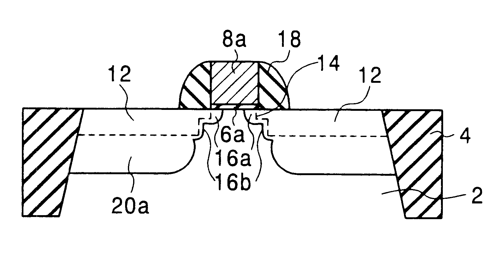
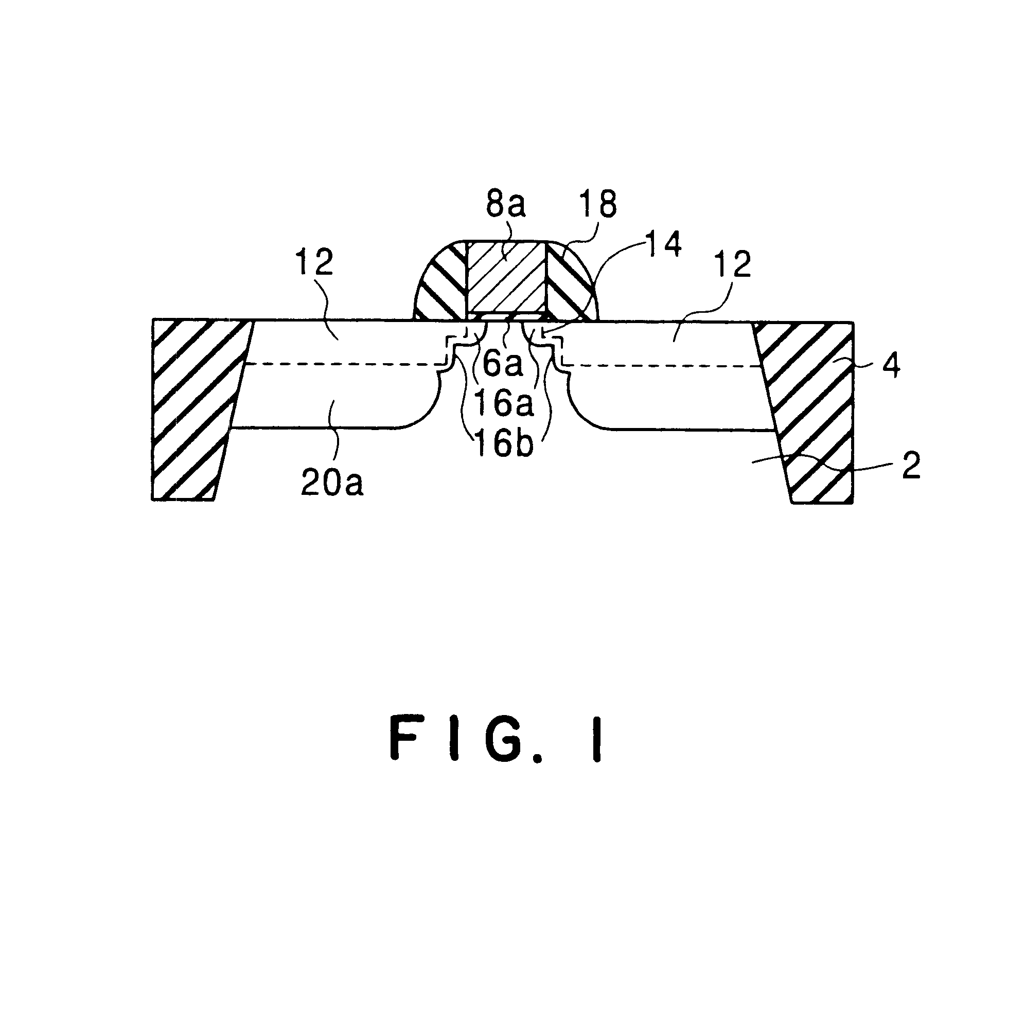
FIG. 1 shows the structure of a semiconductor device according to a first embodiment of the present invention. The semiconductor device of this embodiment includes a p-channel MOSFET having a gate insulating layer 6a formed on an n-type silicon semiconductor region 2 isolated by device isolating regions 4, a gate electrode 8a formed on the gate insulating layer 6a, a channel region formed immediately below the gate electrode 8a in the semiconductor region 2, source / drain regions 20a formed at both the sides of the channel region in the semiconductor region 2, diffusion layer regions (extension regions) 16a and 16b formed between the channel region and the source / drain regions 20a and having a lower p-type impurity (e.g., boron) concentration than the source / drain regions 20a, impurity regions 12 and 14 containing germanium as impurity, and a gate sidewall 18 of an insulating material formed at the side portion of the gate electrode 8a.

The impurity regions 12 are fo...

second embodiment

(Second Embodiment)

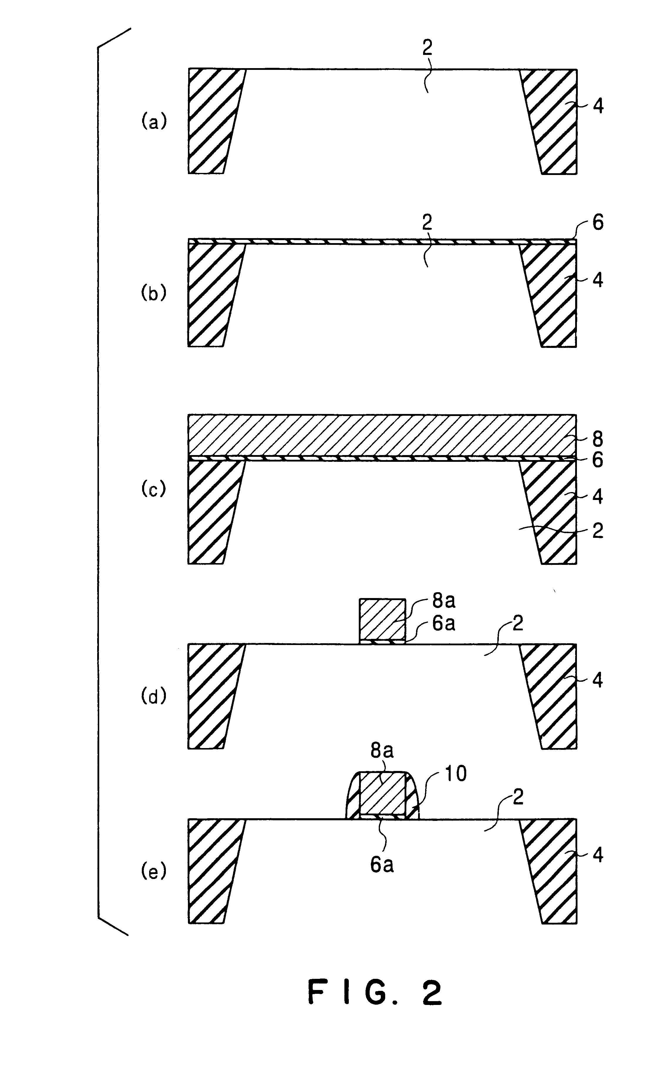
Next, a method of manufacturing a semiconductor device according to a second embodiment of the present invention will be described with reference to FIGS. 2 and 3. The method of this embodiment is for manufacturing the semiconductor device shown in FIG. 1.

First, as shown in FIG. 2(a), the n-type silicon semiconductor region 2, which is isolated by the device isolation regions 4, is formed on the substrate. Then, as shown in FIG. 2(b), an insulating layer 6 is formed on the surface of the semiconductor region 2, and as shown in FIG. 2(c), a polycrystalline silicon layer 8 is grown on the insulating layer 6. Subsequently, the polycrystalline silicon layer 8 and the insulating layer 6 are pattered by the use of the photolithography technique, RIE (Reactive Ion Etching) technique, etc., to form the polycrystalline silicon gate electrode 8a and the gate insulating layer 6a, as shown in FIG. 2(d). Thereafter, as shown in FIG. 2(e), a gate sidewall 10 is formed at the si...


PUM


Abstract

An aspect of the present invention includes: a gate insulating layer formed on an n-type silicon semiconductor region; a gate electrode formed on the gate insulating layer; a channel region formed immediately below the gate electrode in the semiconductor region; p-type source / drain regions formed at both sides of the channel region in the semiconductor region; p-type diffusion layer regions formed between the channel region and the source / drain regions in the semiconductor region and having a lower impurity concentration than the source / drain regions; first impurity regions formed near surface portions of the diffusion layer regions; and second impurity regions formed in part of the p-type diffusion layer regions and near surface portions of the source / drain regions, the second impurity regions being deeper than the first impurity regions, the first and second impurity regions containing one element selected from germanium, silicon, gallium, and indium as impurity.

Description

This application is based upon and claims the benefit of priority from the prior Japanese Patent Application No. 2001-384184, filed on Dec. 18, 2001; the entire contents of which are incorporated herein by reference.1. Field of the InventionThe present invention relates to a semiconductor device and a method of manufacturing the same.2. Related Background ArtRecently, as the miniaturization of devices advances, MOS transistors including diffusion layer regions (hereinafter also referred to as "extension regions"), of which the impurity concentration is lower than that of source / drain regions, have been proposed. In such a MOS transistor, an extension region, of which the junction depth with a semiconductor substrate or a well is shallow, is required for improving the short channel effect, and an extension region, of which the change in impurity concentration per unit length in the direction of the depth of the semiconductor substrate is considerably large, i.e., the impurity concent...

Claims


Application Information

Patent Timeline
Patent Type & Authority Patents(United States)
IPC IPC(8): H01L21/265H01L21/336H01L29/66H01L29/78H01L21/02
CPCH01L21/26506H01L29/6659H01L29/7833H01L21/26513H01L21/2658
Inventor ADACHI, KANNA
Owner KK TOSHIBA
Why Eureka
Try Eureka