Light emitting device and fabricating method thereof

a technology of light-emitting devices and fabrication methods, which is applied in the testing/measurement of individual semiconductor devices, semiconductor/solid-state devices, instruments, etc., can solve the problems of increased manufacturing costs, reduced yield, and complicated manufacturing process to provide

Inactive Publication Date: 2004-03-16
SEMICON ENERGY LAB CO LTD
View PDF26 Cites 94 Cited by
  • Summary
  • Abstract
  • Description
  • Claims
  • Application Information

AI Technical Summary

Benefits of technology

In order to achieve the above objects, the light emitting device according to the present invention is characterized with a gate electrode comprising a plurality of layers each with a different kind of conductive film, and the conductive films with respectively different thicknesses are provided by making use of their selectivity in etching and are used as masks for adjusting concentrations of impurity regions formed in an active layer. The above reduces the number of photolithography steps in relation to manufacturing the TFT for improving yield of the light emitting device and shortening manufacturing term thereof.

Problems solved by technology

However, it makes a manufacturing process complicated to provide the TFT for each of the pixels, and there are caused problems of reduction in yield and increase in manufacturing cost due to a protracted manufacturing term.
Nevertheless, this requires only five times of the photolithography steps.

Method used


Image

  • Light emitting device and fabricating method thereof
  • Light emitting device and fabricating method thereof
  • Light emitting device and fabricating method thereof

Examples


an embodiment 1

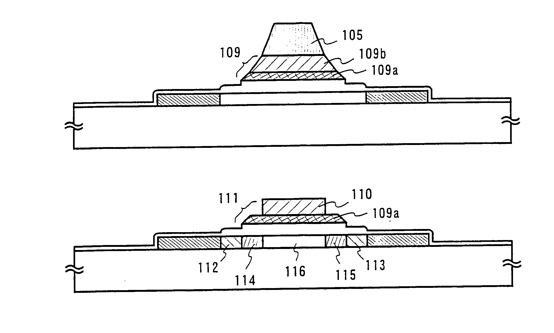
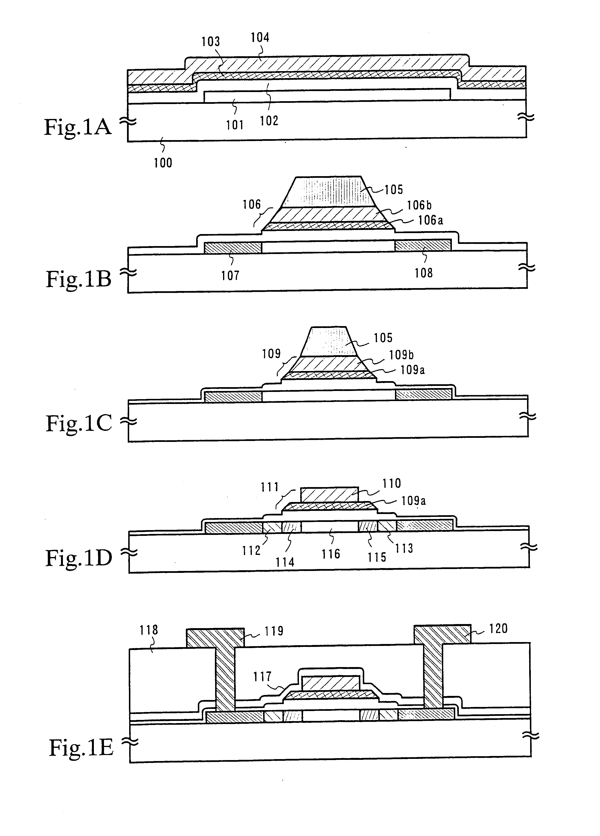
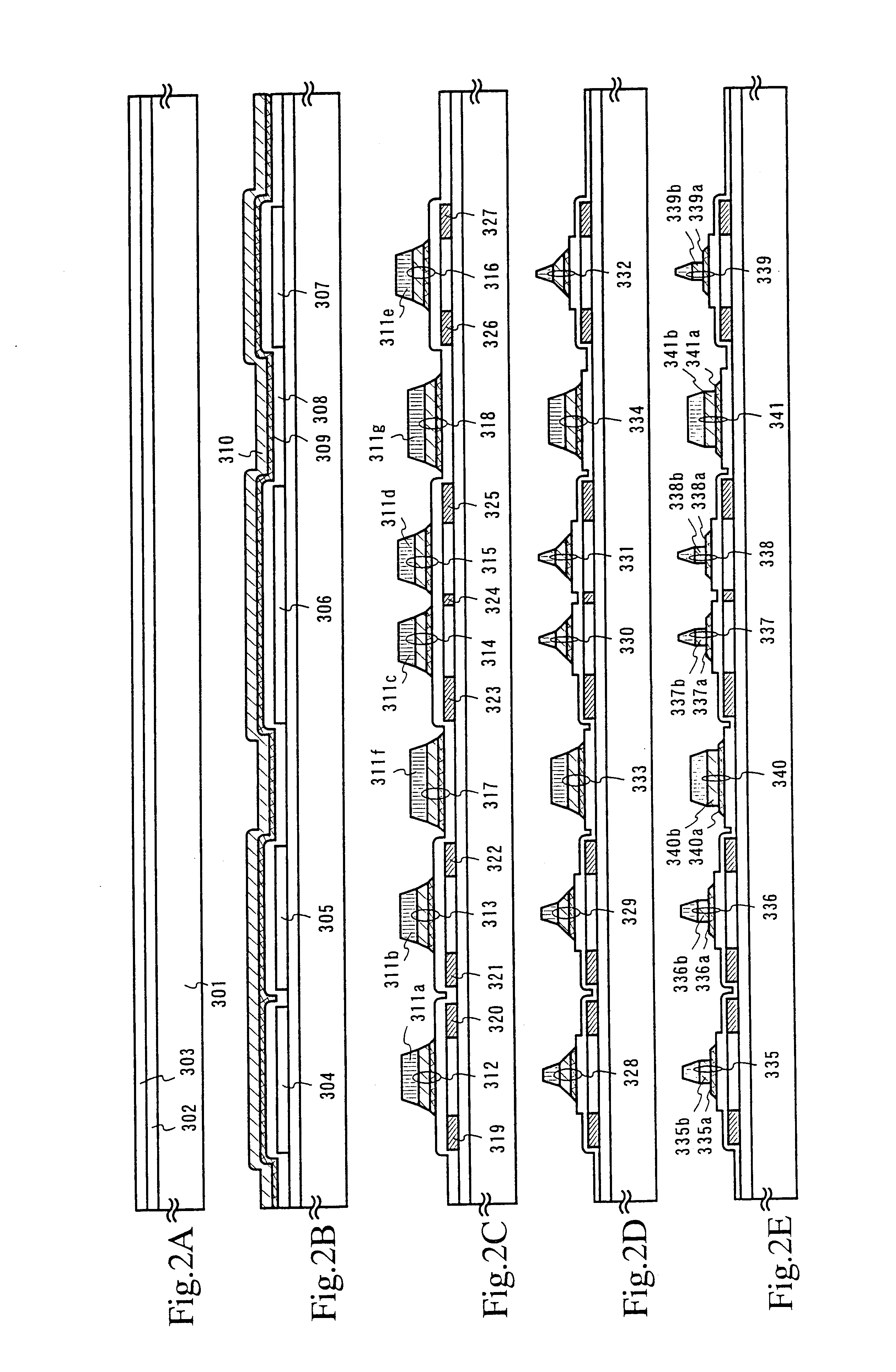
according to the present invention will be explained with reference to FIG. 2A through FIG. 4B. Here, an explanation will be made about a method of simultaneously manufacturing a TFT of a pixel portion and a TFT of a driver circuit provided in the periphery of the pixel portion. For simplifying the explanation a CMOS circuit as a basic unit of the circuit will be shown with respect to driver circuit.

First, as shown in FIG. 2A, a base film 302 is formed of a thickness of 300 nm on a glass substrate 301. In the embodiment 1, silicon oxynitride films are laminated for being used as the base film 302. At this time, nitrogen concentrations in the base film 302 on the side in contact with the glass substrate 301 are better taken as 10 to 25 wt %.

It is effective for the base film 302 to be provided with a heat dissipation effect. Thus, a carbon film, in particular a DLC (diamond-like carbon) film, is effectively provided on each or either side of the substrate 301. The DLC film can be depo...

embodiment 2

In the embodiment 2, an example of arranging the coloring layer is explained using FIG. 10. What is shown in FIG. 10 is a view of the pixel portion seen from above. The structure of each of the pixels is same as that explained using FIG. 5 and FIG. 6A to FIG. 6C.

In FIG. 10, reference numerals 1201, 1202, and 1203 denote a red coloring layer, a green coloring layer, and a blue coloring layer, respectively. Moreover, reference numerals 1204, 1205, and 1206 are pixels for emitting blue color, green color, and red color, respectively. Here, in the embodiment 2, the pixel 1204 for blue color is provided with the blue coloring layer 1203, the pixel 1205 for green color is provided with the green coloring layer 1202, and the red coloring layer 1201 is provided above the pixel 1206 for red color and each TFT. The red coloring layer 1201 has an opening portion 1208 at each contact portion 1207.

The crystalline silicon film made to be the active layer of the TFT has a characteristic that an ab...

embodiment 3

In the embodiment 1, an example is presented, in which an EL material, from which emission of white light can be obtained, is used as the light emitting layer. The white light emitted is then made to pass through the red coloring layer, the green coloring layer, and the blue coloring layer to obtain red light, green light, and blue light, respectively.

In the embodiment 3, unlike the embodiment 1. Light emitting layers, from which red light, green light, and blue light can be obtain, are formed in pixels for red, green, and blue, respectively. The red light, the green light, and the blue light emitted from the respective light emitting layers are made to pass through the red coloring layer, the green coloring layer, and the blue coloring layer, respectively, to improve purity of each color.

In the embodiment 3, it is necessary to deposit three kinds of EL materials which respectively emit red, green and blue. However, known materials can be used. In addition, it is also necessary to c...


PUM


Abstract

The light emitting device according to the present invention is characterized in that a gate electrode comprising plurality of conductive films is formed, and concentration of impurity regions in an active layer are adjusted with making use of selectivity of the conductive films in etching and using them as masks. The present invention reduces the number of photolithography steps in relation to manufacturing the TFT for improving yield of the light emitting device and shortening manufacturing term thereof, by which a light emitting device and an electronic appliance are inexpensively provided.

Description

1. Field of the InventionThe present invention relates to a light emitting device which has an element with a luminescent material put between electrodes, a manufacturing method thereof, and an electronic appliance using the light emitting device for the display (an indication display or a displaying monitor), particularly to a light emitting device using a luminescent material by which EL (Electro Luminescence) can be obtained (hereinafter referred to as an EL material) and a manufacturing method thereof. The light emitting device according to the present invention includes an organic EL display and an OLED (Organic Light Emitting Diode).The luminescent material that can be used in the present invention includes all of materials which emit light (phosphorescence and / or fluorescence) through singlet excitation, triplet excitation, or both.2. Description of the Related ArtRecently, there has been proceeding development of light emitting devices (hereinafter referred to as EL light em...

Claims


Application Information

Patent Timeline
Patent Type & Authority Patents(United States)
IPC IPC(8): H01L21/336H01L29/423H01L29/40H01L21/02H01L27/12H01L21/70H01L29/49H01L21/84H01L21/77
CPCH01L27/1214H01L29/42384H01L29/4908H01L29/66757H01L27/1288H01L27/124H01L27/127
Inventor YAMAZAKI, SHUNPEIFUKUNAGA, TAKESHIKOYAMA, JUNINUKAI, KAZUTAKA
Owner SEMICON ENERGY LAB CO LTD
Why Eureka
Try Eureka