Method and device for measuring luminescence

a luminescence and luminescence technology, applied in the direction of fluorescence/phosphorescence, optical radiation measurement, instruments, etc., can solve the problems of complicated technical design, inability to measure very low detection concentrations, and limited use of essentially coherent light in order

Inactive Publication Date: 2004-03-23
NOVARTIS AG
View PDF11 Cites 56 Cited by
  • Summary
  • Abstract
  • Description
  • Claims
  • Application Information

AI Technical Summary

Problems solved by technology

The use of adjusting components is therefore mandatory, and this complicates the technical design and is evident, in particular, in the case of the construction of arrays.
In addition, one is limited to the use of essentially coherent light in order to coordinate the positioning with the constants of the incoupling elements and such as, for example, diffractive gratings.
Such thick glass substrates used as multimodal waveguides are not suitable for measuring very low detection concentrations.
An evanescent luminescence excitation with the aid of UV light and the use of planar waveguides with incoupling elements is possible only to a limited extent, since grating periods of below 300 nm for coupling in the UV radiation can be produced only at great expense and, moreover, UV radiation is very strongly damped in the waveguide.
Furthermore, the interruption of the waveguiding layer can already be achieved using masks during the application of the waveguiding layer.
If a numerically very large array of sensor elements, for example, 100 or more sensor elements, is to be illuminated simultaneously, the intens...

Method used


Image

  • Method and device for measuring luminescence
  • Method and device for measuring luminescence
  • Method and device for measuring luminescence

Examples


Embodiment Construction

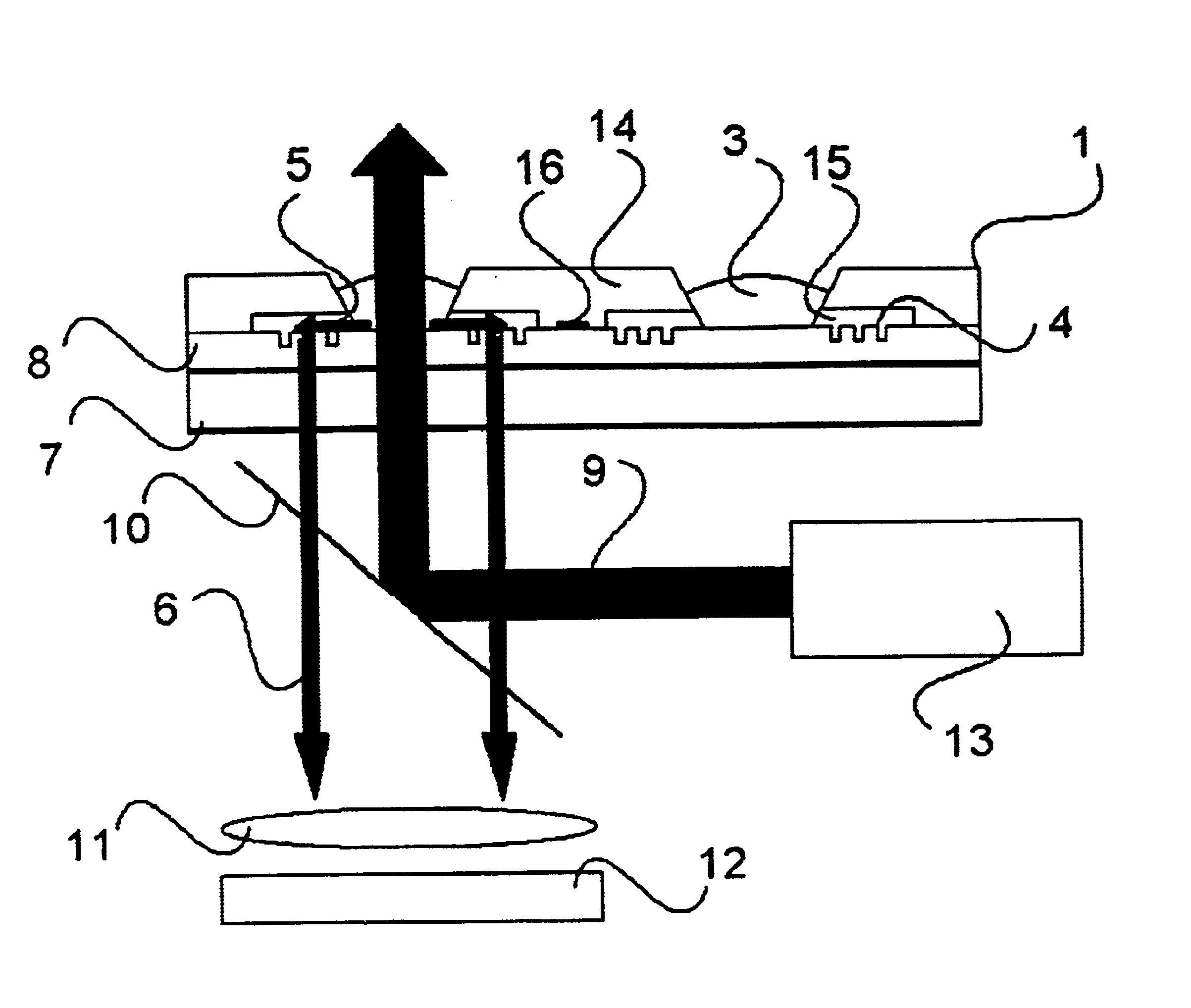
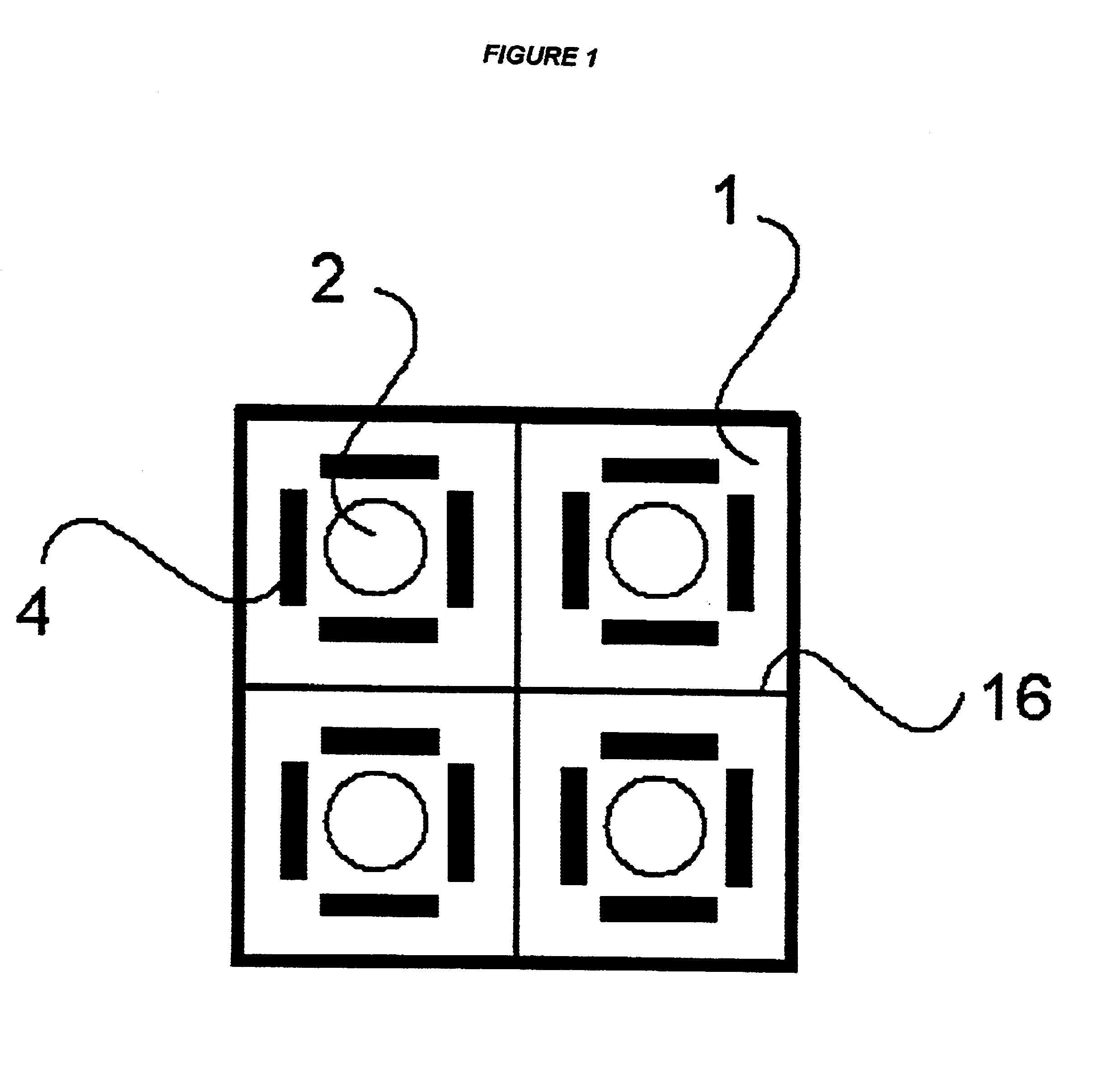
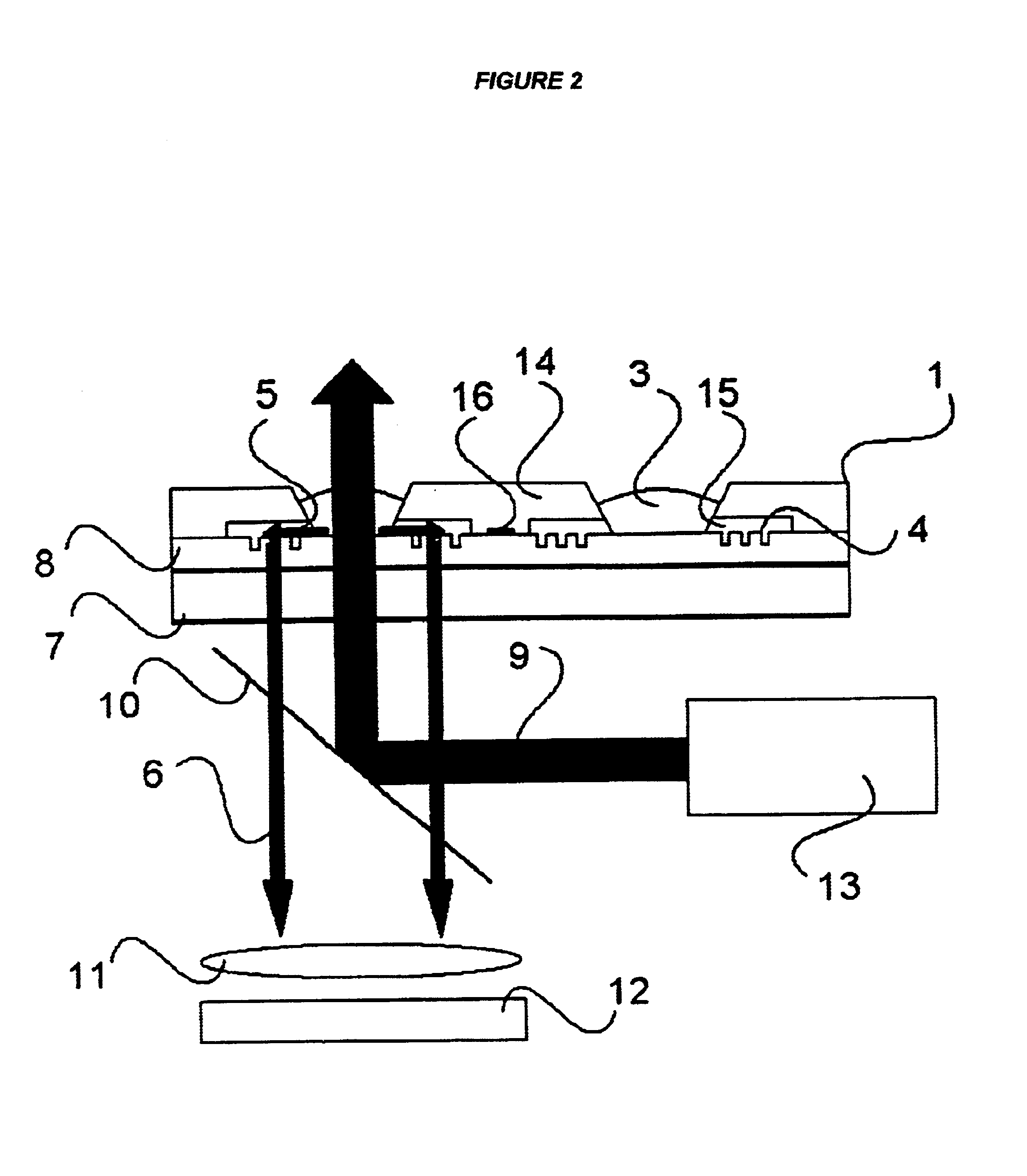
The effectiveness of the excitation method in the volume of an analyte sample 3 is tested with the aid of a DNA hybridizing assay. The waveguide consists of Corning glass C7059 as substrate material 7 and Ta.sub.2 O.sub.5 as waveguiding layer 8 (layer thickness 150 nm), and contains two outcoupling gratings 5 with a modulation transfer factor of approximately 10 nm and a grating period of 320 nm. The cutout for the analyte sample is located in the middle of the grating at a distance of 5 mm. In order to immobilize oligonucleotide detection elements, the waveguiding surface is silanized with 3-glycidoxypropyltrimethoxysilane in the liquid phase (ortho-xylene). The following oligonucleotide is covalently immobilized as a detection element on the functionalized silane layer with a typical occupation density of 10%. Amino-(C6bridging group)5'-CACAATTCCACACAAC-3'. The covalent bonding of the oligonucleotide is performed via the free amino group of the oligonucleotide and the epoxide grou...


PUM


Abstract

A method exites and determines a luminescence in an analyte sample which is located in contact with the waveguiding layer of an optical layer waveguide. The luminescence is generated by non-evanescent excitation in the volume of the analyte sample. Luminescence radiation generated in the immediate proximity of the surface of the waveguiding layer is conducted to a measuring device and determined after penetrating the waveguiding layer.

Description

1. Field of the InventionThe invention relates to a method for exciting and determining a luminescence of an analyte which is located in contact with a surface of a waveguiding layer of a layer waveguide. In a case of which, a luminescence is generated in a non-evanescent way in the volume of the analyte which leads to an optical measuring device from the immediate proximity on the surface of the waveguiding layer luminescence radiation which has penetrated into the waveguiding layer of the layer waveguide, preferably via at least one outcoupling element for the luminescence radiation. Then, the optical measuring device measures the luminescence light, for example, optoelectronically. The invention also relates to a measuring device for carrying out the method, and to a sensor platform.2. Description of the Related ArtIn affinity sensor technology, biochemical detection elements are immobilized on a waveguide surface either directly or via an adhesion promoter layer, for the purpose...

Claims


Application Information

Patent Timeline
IPC IPC(8): G01N21/77G01N21/76G01N21/64G01N21/66G01N33/483
CPCG01N21/7703G01N21/76G01N21/6452G01N21/69
Inventor MAROWSKY, GERDNEUSCHAEFER, DIETERPAWLAK, MICHAEL
Owner NOVARTIS AG
Why Eureka
Try Eureka