Solid state image sensor and method for fabricating the same

a solid-state image and sensor technology, applied in the direction of television system scanning details, radio frequency control devices, television systems, etc., can solve the problems of microlenses formed of transparent resinous materials that are susceptible to deformation, difficult spherical surface control of microlenses,

Inactive Publication Date: 2004-04-20
INTELLECTUAL VENTURES II
View PDF9 Cites 31 Cited by
  • Summary
  • Abstract
  • Description
  • Claims
  • Application Information

AI Technical Summary

Problems solved by technology

First, spherical surface control of the microlenses is difficult, and dependent on process parameters.
Second, as a contact depth of the PDs becomes greater, a depth of focus cannot be made

Method used


Image

  • Solid state image sensor and method for fabricating the same
  • Solid state image sensor and method for fabricating the same
  • Solid state image sensor and method for fabricating the same

Examples


first embodiment

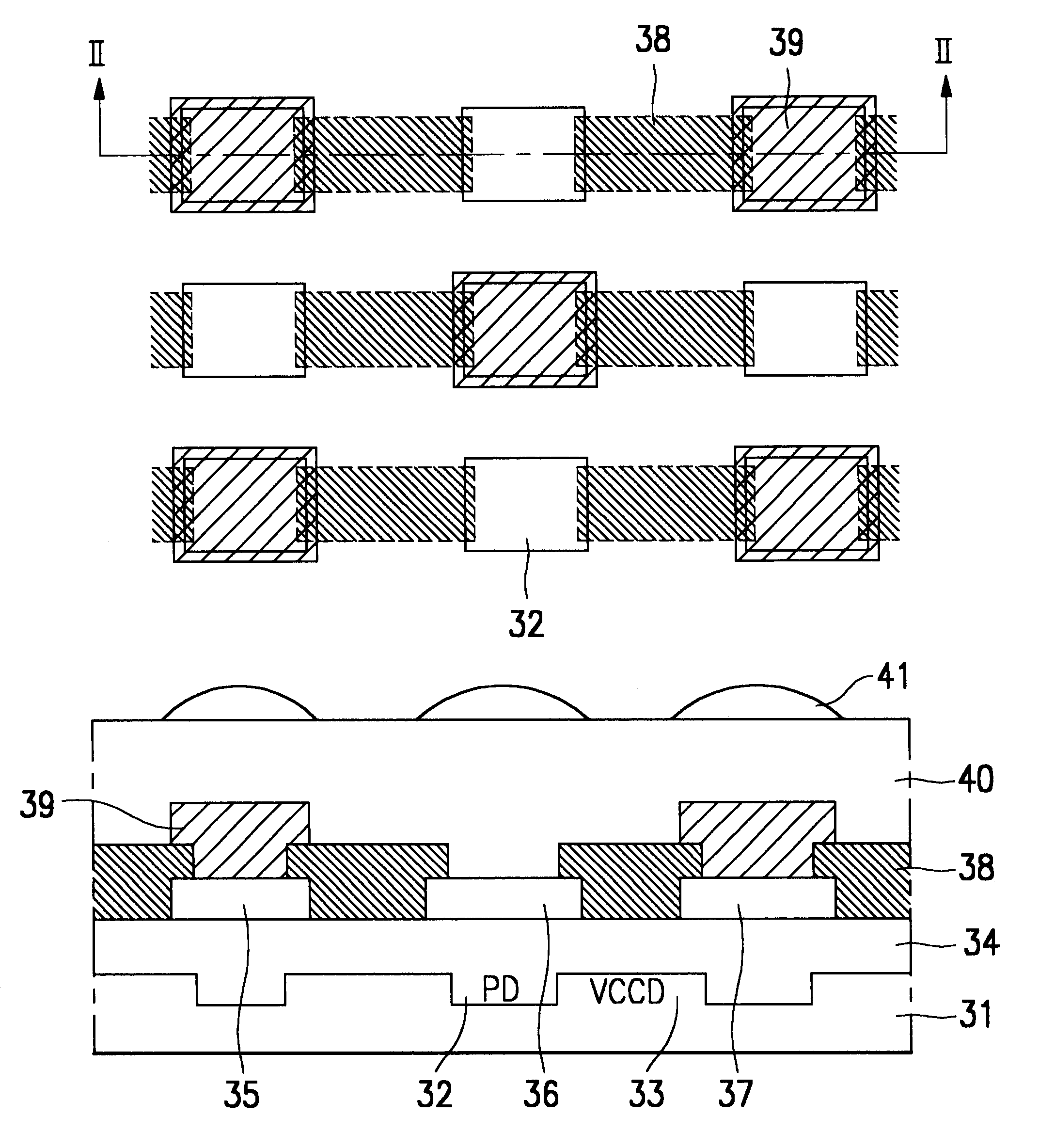
FIG. 2a is a plan view of a solid state image sensor according to the present invention and FIG. 2b is a cross-sectional view taken along the line II--II of FIG. 2a.

As illustrated in FIGS. 2a and 2b, the solid state image sensor according to a first embodiment of the present invention includes a first flat layer 34 formed on a black-and-white solid state image sensor 31, which includes a plurality of PDs 32 arranged in a matrix for converting image signals of light to electrical signals, vertical CCDs 33 for transmitting image charges generated in the PDs 32 in the vertical direction, and a horizontal CCD (not shown) for transmitting the vertically transmitted image charges in the horizontal direction, first to third color filter layers 35, 36 and 37 formed on the first flat layer 34 to be in correspondence to the PDs 32 on a one-to-one basis, a plurality of black layers 38 of a chrome (Cr) film or a titanium nitride (TiN) film on the first flat layer 34 between the first to third c...

second embodiment

FIGS. 5a-5d are cross-sectional views illustrating the steps of a method for fabricating the solid state image sensor according to the present invention.

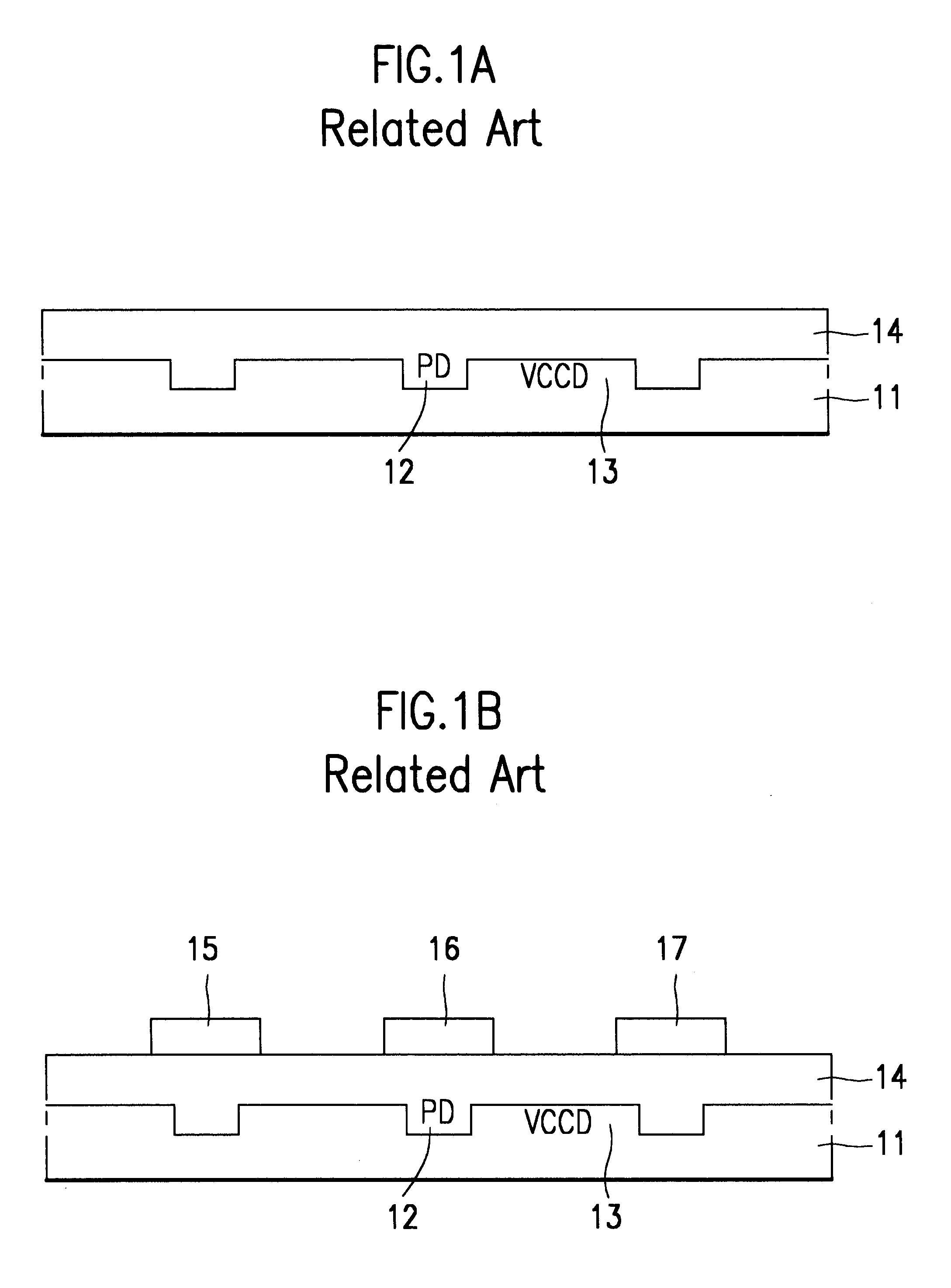
As shown in FIG. 5a, the first flat layer 34 is formed on the black-and-white solid state image sensor 31, which includes a plurality of PDs 32 for converting image signals of light to electrical signals, vertical CCDs 33 for transmitting image charges generated in the PDs 32 in a vertical direction, and a horizontal CCD (not shown) for transmitting the vertically transmitted image charges in the horizontal direction.

As shown in FIG. 5b, first to third color filter layers 35, 36 and 37 are selectively formed on the first flat layer 34 in succession to be in correspondence to the PDs 32 on a one-to-one basis. The color filter layers are formed by coating and patterning a colorable resist and then dying and fixing the patterned colorable resist.

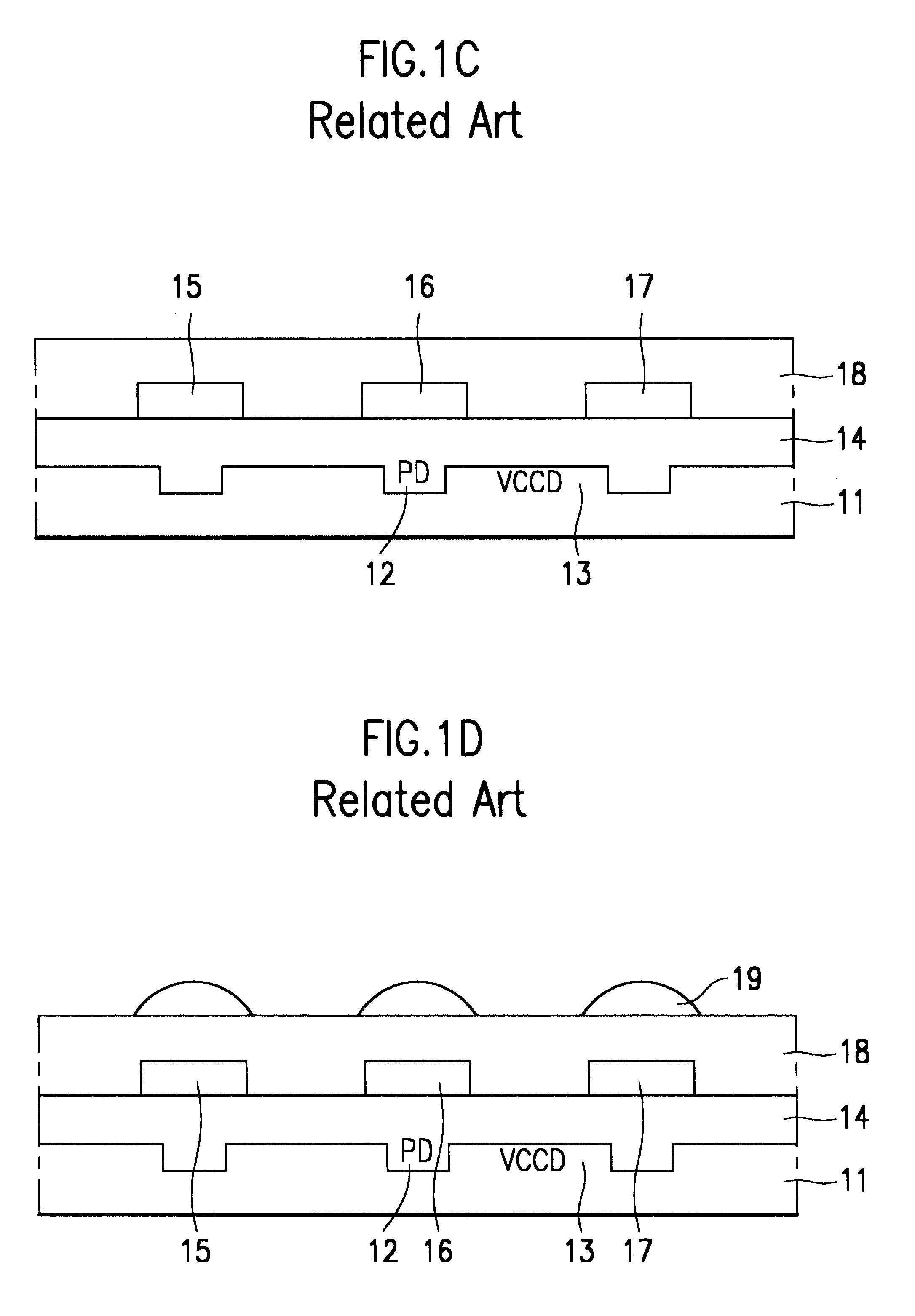
As shown in FIG. 5c, a second flat layer 40 is formed on an entire surface including the fi...

third embodiment

FIG. 6 is a cross-sectional view of a solid state image sensor according to the present invention.

As illustrated in FIG. 6, the solid state image sensor according to a third embodiment of the present invention includes a black-and-white solid state image sensor 31, which includes a plurality of PDs 32 arranged at fixed intervals in a matrix for converting image signals of light to electrical signals, vertical CCDs 33 for transmitting image charges generated in the PDs 32 in a vertical direction, and a horizontal CCD (not shown) for transmitting the vertically transmitted image charges in the horizontal direction. There is a gate insulating layer 43 formed on the black-to-white solid state image sensor 31 and a transfer gate 44 formed on the gate insulating layer 43 on the top of the vertical CCDs 33 for changing the potential of the transfer gate 44 according to clock signals. And, there is a metallic shielding layer 46 formed to surround the transfer gate 44 for preventing infiltra...


PUM


Abstract

Solid state image sensor suitable for enhancing sensitivity of charge coupled devices (CCDs) using phase shift of light, and method for fabricating the same, the solid state image sensor including a plurality of photodiodes for generating image charges from incident lights, a plurality of charge coupled devices provided between the photodiodes for transmitting the image charges in one direction, a first flat layer formed on an entire surface of the photodiodes and the charge coupled devices, a plurality of color filter layers formed on the first flat layer to be in correspondence to the photodiodes, a plurality of black layers formed on the first flat layer between the color filter layers, a plurality of phase shift layers selectively formed on the color filter layers to be in correspondence to the photodiodes alternately, a second flat layer formed on an entire surface including the phase shift layers, and a plurality of microlenses formed on the second flat layer to be in correspondence to the photodiodes.

Description

1. Field of the InventionThe present invention relates to a solid state image sensor and, more particularly to, a solid state image sensor suitable for enhancing sensitivity of charge coupled devices (CCDs) using phase shift of light, and a method for fabricating the same.2. Background of the Related ArtIn general, a solid state image sensor refers to a device for image sensing an object and converting the image to electrical signals using photoelectric conversion elements and charge coupled elements.The charge coupled elements are used to transmit signal charges generated in the photoelectric conversion elements (i.e., photodiodes) passed through a color filter layer in a specified direction through a microlens using variations of electric potential in a substrate.The solid state image sensor includes a plurality of photodiodes (PDs), vertical CCDs each provided between the PDs for transmitting charges generated from the PDs in the vertical direction, horizontal CCDs for transmitti...

Claims


Application Information

Patent Timeline
IPC IPC(8): H04N5/225H01L27/146H01L27/148
CPCH01L27/14621H01L27/14623H01L27/14627H01L27/14632H01L27/14685H01L27/14687H01L27/14806H04N5/2254H01L27/146H01L27/148
Inventor MOON, SANG HOCHOI, IN KYOU
Owner INTELLECTUAL VENTURES II
Why Eureka
Try Eureka