Controlling a delay lock loop circuit

a delay lock and circuit technology, applied in the direction of digital storage, pulse automatic control, instruments, etc., can solve the problems of semiconductor memory to malfunction, device density is very high, and it is difficult to isolate the device and/or line completely,

Inactive Publication Date: 2004-04-27
MICRON TECH INC
View PDF8 Cites 139 Cited by
  • Summary
  • Abstract
  • Description
  • Claims
  • Application Information

AI Technical Summary

Problems solved by technology

These devices are very densely packed, i.e., there is little space between them.
Although forming the selected electrical connections may enable the circuits to perform their intended functions, undesirable electrical connections may result in a variety of malfunctions, e.g., short circuit paths may be established.
However, it may be difficult to completely isolate the devices and / or lines.
For example, defects in the semiconductor substrate or in the manufacturing process may form an undesirable conducting path between the devices and / or lines in the semiconductor memory that may cause the semiconductor memory to malfunction.
The problems associated with the current methodologies of implementing the delay lock loop include an overreaction when performing delay compensation due to external factors on a digital line.
These external factors that cause inadvertent adjustments of the delay lock loop include a noise spike on a bus or a control signal.
These noise spikes may cause a delay lock loop circuit to be over-dynamic, wherein the delay lock loop circuit tracks a noise spike, thereby adding unintentional delays to the line.

Method used


Image

  • Controlling a delay lock loop circuit
  • Controlling a delay lock loop circuit
  • Controlling a delay lock loop circuit

Examples


Embodiment Construction

Illustrative embodiments of the invention are described below. In the interest of clarity, not all features of an actual implementation are described in this specification. It will of course be appreciated that in the development of any such actual embodiment, numerous implementation-specific decisions must be made to achieve the developers' specific goals, such as compliance with system-related and business-related constraints, which will vary from one implementation to another. Moreover, it will be appreciated that such a development effort might be complex and time-consuming, but would nevertheless be a routine undertaking for those of ordinary skill in the art having the benefit of this disclosure.

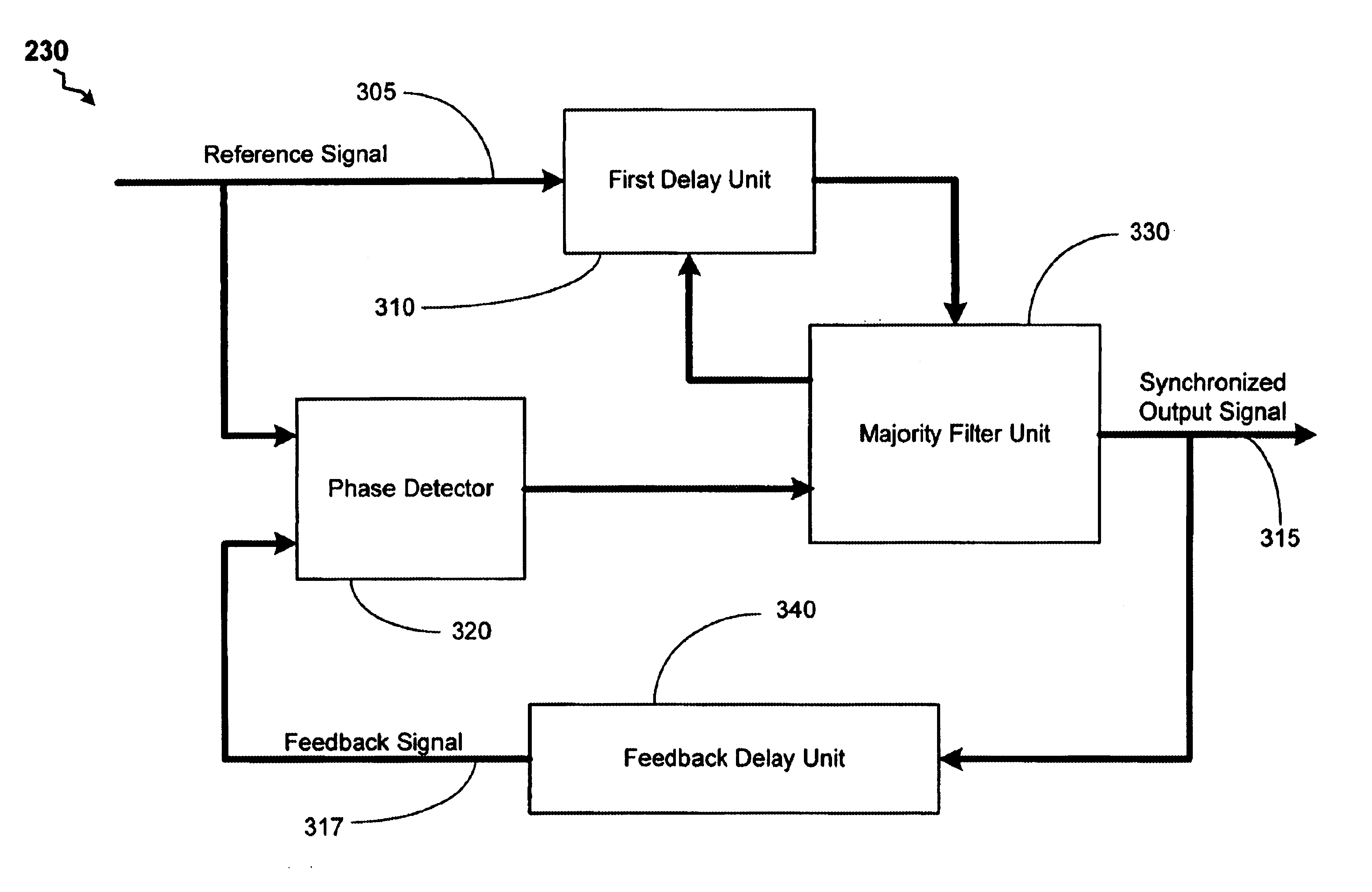
Synchronization between multiple digital signals in a digital system is important for accurate exchange of digital data. Often, delay lock loops are employed to synchronize digital signals. However, without a signal filtering system, the delay lock loop may cause overreaction to extern...


PUM


Abstract

A method and apparatus is provided for performing a filter control of a delay lock loop circuit. A coarse delay and / or a fine delay are implemented upon a reference signal based upon a phase shift between the reference signal and a feedback signal. A synchronized output signal is generated based upon the coarse delay and the fine delay. The apparatus of the present invention includes a delay lock loop to provide an output signal based upon a phase difference between a reference signal and a feedback signal. The delay lock loop comprises a filter to provide a filter response to the phase difference. The filter response is capable of providing a coarse delay and / or a fine delay.

Description

1. Field of the InventionThis invention generally relates to a semiconductor memory device, and, in particular, to a majority filter control of a delay lock loop.2. Description of the Related ArtModem integrated circuit devices are comprised of millions of semiconductor devices, e.g., transistors, formed above a semiconductor substrate, such as silicon. These devices are very densely packed, i.e., there is little space between them. Similarly densely packed electrically conducting lines may also be formed in the semiconductor substrate. By forming selected electrical connections between selected semiconductor devices and selected conducting lines, circuits capable of performing complex functions may be created. For example, bits of data may be stored by providing electrical current to a plurality of bit lines and an orthogonal plurality of word lines that may be electrically coupled to one or more capacitors in a semiconductor memory.The semiconductor memory may be a dynamic random ...

Claims


Application Information

Patent Timeline
Patent Type & Authority Patents(United States)
IPC IPC(8): H03L7/08H03L7/081
CPCH03L7/0814H03L7/0818H03L7/0816
Inventor GOMM, TYLER J.DERMOTT, ROSS E.
Owner MICRON TECH INC
Why Eureka
Try Eureka