Substrates having increased thermal conductivity for semiconductor structures

a technology of semiconductor structure and thermal conductivity, which is applied in the direction of semiconductor laser structure details, semiconductor lasers, lasers, etc., can solve the problems of inefficient heat flow out poor and increase in temperature detrimental to the performance of the semiconductor devi

Inactive Publication Date: 2004-06-01
XEROX CORP
View PDF3 Cites 21 Cited by
  • Summary
  • Abstract
  • Description
  • Claims
  • Application Information

AI Technical Summary

Benefits of technology

The inventors have discovered that, if there is a region formed of a material having enhanced thermal conductivity connecting the light emitting devices to the external heat sink, then the heat will flow out of the device along the path created by that material. As a result, the temperature of the device will depend less on the dissipated power of the adjacent devices. Thus, having materials with enhanced thermal conductivity between the active region of a device and the external heat sink will lead to lower temperatures during operation and to improved stability of operation. In many instances, such as with multiple monolithically integrated laser diodes, the thermal cross-talk between devices will also be reduced.

Problems solved by technology

Some semiconductor devices experience poor performance because the heat that is generated during operation is not able to flow out of the semiconductor device efficiently.
This leads to an increase in temperature that is detrimental to the performance of the semiconductor device.
The inefficient heat flow out of the semiconductor device is often attributable to those parts of the device that have low thermal conductivity.
However, to reach the heat sink, the heat must often flow through a region of the device that has a low thermal conductivity.
This occurs because the temperature in the first device is affected by the amount of dissipated power, and therefore the amount of heat, that is generated by the adjacent devices.
For many applications, e.g., laser printing, cross-talk between adjacent light emitting devices is highly undesirable, because the light emitting devices are desirably separately addressable and completely independent from each other.
However, when using conventional techniques like polishing, a further reduction in substrate thickness is difficult to achieve without cracking the substrate.
As a result, such thinning procedures have not been satisfactory to reduce heating.
Copper, however, is not suitable as a substrate for growth of semiconductors, because its melting temperature is lower than the high temperatures required for growth of these materials.

Method used


Image

  • Substrates having increased thermal conductivity for semiconductor structures
  • Substrates having increased thermal conductivity for semiconductor structures
  • Substrates having increased thermal conductivity for semiconductor structures

Examples


second embodiment

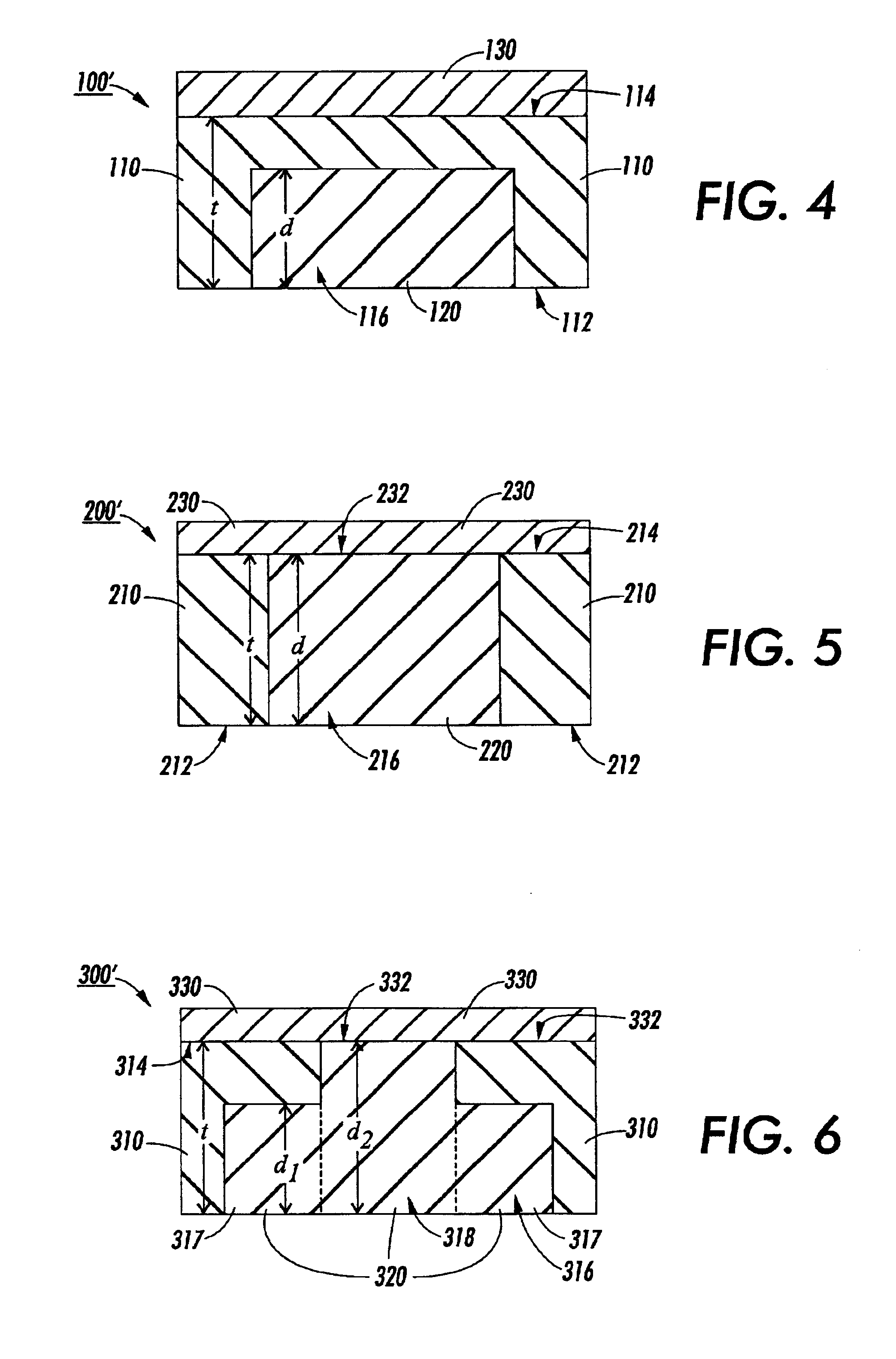
In various other exemplary embodiments, such as the second embodiment illustrated in FIG. 5, a semiconductor device 200' includes the substrate 200 according to this invention, as illustrated in FIG. 2 and described above. A semiconductor structure 230 is formed over the top surface 214 of the substrate 200.

The cavity 216 opens onto the top surface 214 and the bottom surface 212. The material 220 contacts a bottom surface 232 of the semiconductor structure 230.
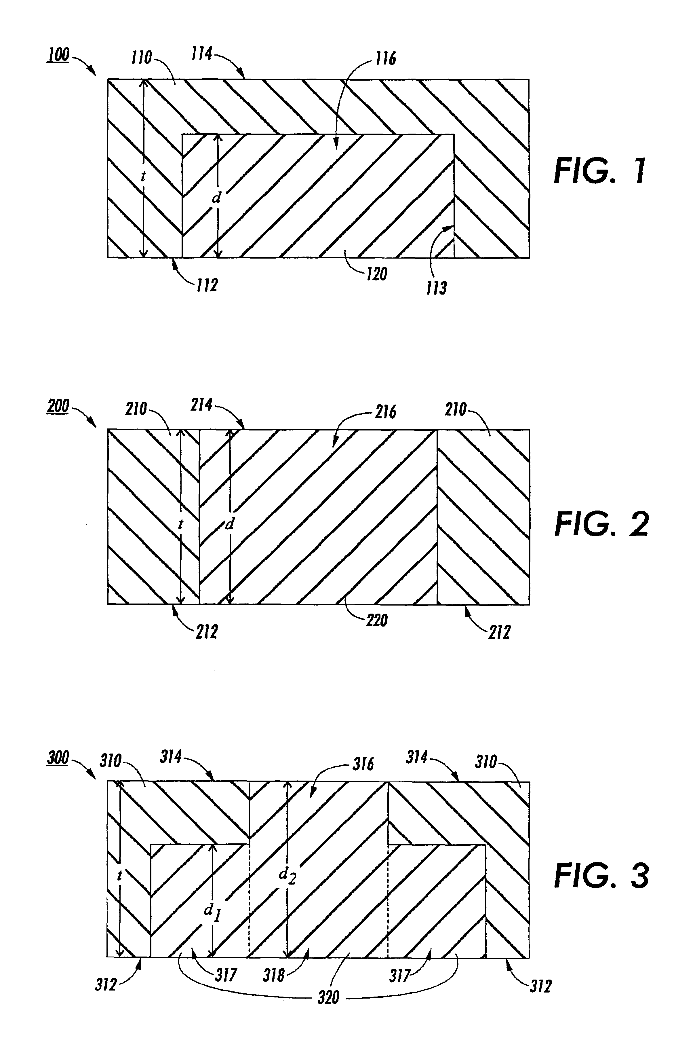
third embodiment

In various other exemplary embodiments, such as the third embodiment illustrated in FIG. 6, a semiconductor device 300' includes the substrate 300 according to this invention having the cavity 316 with a stepped configuration, as illustrated in FIG. 3 and described above. A semiconductor structure 330 is formed over the top surface 314. The cavity 316 opens onto the top surface 314 and the bottom surface 312. The material 320 contacts a bottom surface 332 of the semiconductor structure 330.

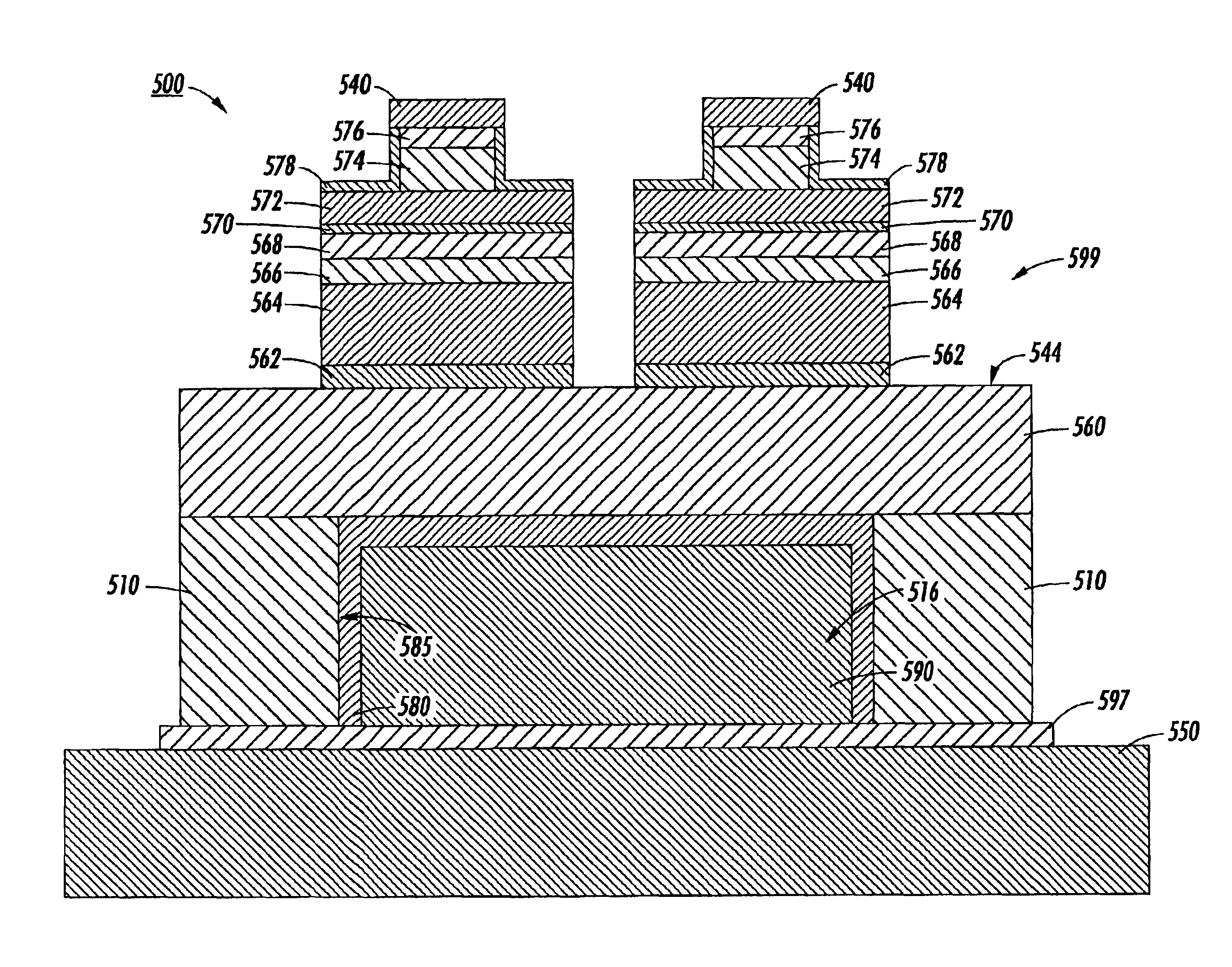
Various exemplary embodiments of the semiconductor devices according to this invention further include at least one p-contact and at least one n-contact. In a fourth exemplary embodiment of the semiconductor device 100", as illustrated in FIG. 7, the semiconductor device includes at least one p-contact 140 and at least one n-contact 144. The p-contacts 140 are in contact with the semiconductor structure 130. The n-contact 144 is also in contact with the semiconductor structure 130. A heat sink 150...


PUM

PropertyMeasurementUnit
thicknessaaaaaaaaaa
widthaaaaaaaaaa
widthaaaaaaaaaa

Abstract

Substrates having increased thermal conductivity are provided, comprising a body having opposed surfaces and a cavity that opens on at least one surface, the cavity containing at least one material having a greater thermal conductivity than the body. Devices are provided comprising a substrate and a semiconductor over a surface of the substrate. Methods of forming devices according to the invention are also provided.

Description

1. Field of InventionThis invention is directed to semiconductor devices that have reduced thermal resistance.2. Description of Related ArtSome semiconductor devices experience poor performance because the heat that is generated during operation is not able to flow out of the semiconductor device efficiently. This leads to an increase in temperature that is detrimental to the performance of the semiconductor device. In many cases the temperature rise (.DELTA.T) is proportional to the heat per unit time (.DELTA.W) that is generated by the semiconductor device, i.e., .DELTA.T=R.DELTA.W. Here, the proportionality factor R is the thermal resistance of the semiconductor device.The inefficient heat flow out of the semiconductor device is often attributable to those parts of the device that have low thermal conductivity. In some semiconductor devices, during operation, heat must flow from the point where the heat is generated to an external heat sink. The heat sink has a sufficiently large...

Claims


Application Information

Patent Timeline
Patent Type & Authority Patents(United States)
IPC IPC(8): H01L29/02H01L23/367H01L23/34H01L33/00H01L29/06H01S5/00H01S5/02H01S5/024H01L27/15H01L23/36H01L33/64
CPCB82Y20/00H01L23/3677H01L29/0657H01L33/642H01S5/02484H01S5/3202H01S5/0213H01L27/15H01S5/0207H01L2924/10158H01S5/02469H01S5/34333H01L2224/32H01S5/0202H01S5/026H01S5/04257H01S5/4031H01S5/02461
Inventor ROMANO, LINDA T.KNEISSL, MICHAEL A.NORTHRUP, JOHN E.
Owner XEROX CORP
Why Eureka
Try Eureka