Method of reducing the propagation delay and process and temperature effects on a buffer

a technology of applied in the field of reducing the propagation delay and process temperature effect on the buffer, can solve the problems of extended ringing, system errors, uncontrollable interconnection line impedance loading,

Inactive Publication Date: 2004-06-29
SEMICON COMPONENTS IND LLC
View PDF4 Cites 25 Cited by
  • Summary
  • Abstract
  • Description
  • Claims
  • Application Information

AI Technical Summary

Problems solved by technology

Since the systems and the backplane interconnections are arbitrarily dispersed and/or bussed to a number of different systems, the interconnection line impedance loading is uncontrolled.
In such systems high speed edges may cause system errors.
The uncontrolled termination impedance mismatches and line lengths of the interconnecting transmission lines result in extended ringing with high voltage swings that may interfere with logic functions.
Moreover, the high speed edges will capacitively couple to other signal lines causing errors, and magnetic coupling among signal lines when currents abruptly change due to impedance anomalies also may cause log

Method used


Image

  • Method of reducing the propagation delay and process and temperature effects on a buffer
  • Method of reducing the propagation delay and process and temperature effects on a buffer
  • Method of reducing the propagation delay and process and temperature effects on a buffer

Examples


Embodiment Construction

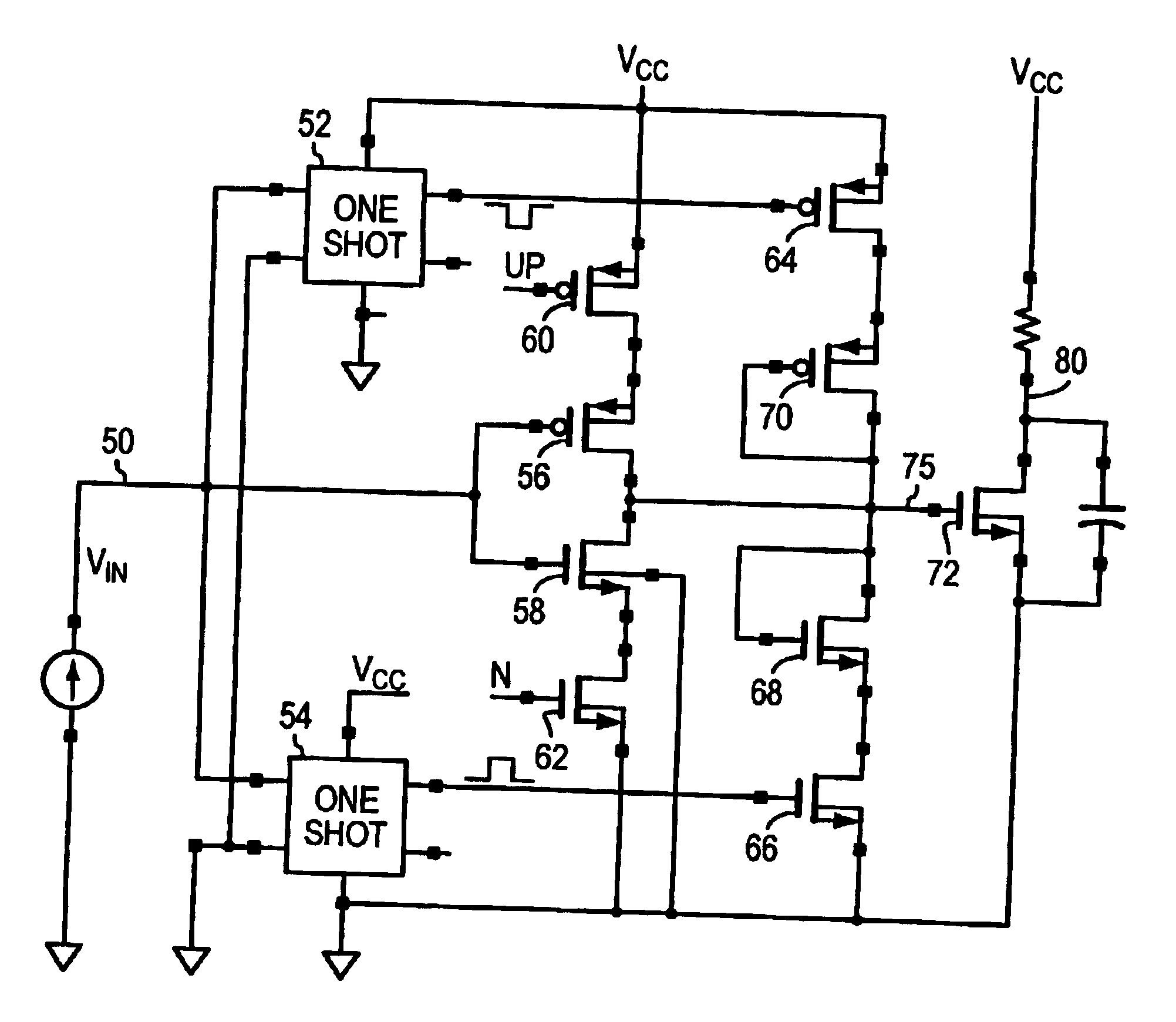
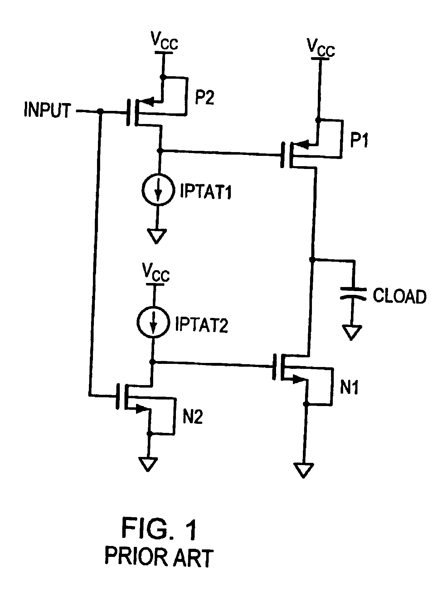
. 3 is a schematic illustrating one embodiment of the present invention. The approach is to supply a short "tug" or pull on the gate of the output transistor in the same direction as the current sources of the prior art FIG. 1. The pull drives the gates quickly up to the output transistor thresholds to counter act the delay that would have occurred had only the low current been available to drive the gates. The pull will not affect the slow output edge if the pull is limited to only overcoming the thresholds, e.g. the first few hundred millivolts at the gates. After traversing these first several hundred millivolts of transition, the low current sources 10 and 12 continue to slowly drive the gate thereby producing the slow output edges desired. The edge transitions depend primarily on this finishing drive and so the slow edges are maintained. The pull starts the output moving well before it would have occurred without the present invention and so reduces the delay without affecting ...


PUM


Abstract

A buffer circuit with slow output edges is described. Pulsed higher value currents are driven from one shot timing circuits to inject a pulse of current into the control gate of the buffer's output MOSFET to speed up the beginning of the turning on or the turning off of the output MOSFT. When the beginning and turning on and off is reached lower value current sources continue to drive the gate of the output MOSFET. In one embodiment, one shots are triggered from the rising and falling edges of the input signal. The effect of the higher value current pulses is to reduce the circuit delay through the buffer. Also, the pulse width can be designed as temperature sensitive, and supply voltage sensitive so as to maintain the buffer circuit delay as substantially constant as temperature, supply voltage and process variation occur.

Description

1. Field of the InventionThe present invention relates to minimizing the effects of temperature and of manufacturing processing on the delay of a buffer while providing a fast buffer circuit propagation delay.2. Background InformationMany electronic systems are built using backplane interconnections arrangement for sharing information and data among the various functions in particular systems. Since the systems and the backplane interconnections are arbitrarily dispersed and / or bussed to a number of different systems, the interconnection line impedance loading is uncontrolled. In such systems high speed edges may cause system errors. The uncontrolled termination impedance mismatches and line lengths of the interconnecting transmission lines result in extended ringing with high voltage swings that may interfere with logic functions. Moreover, the high speed edges will capacitively couple to other signal lines causing errors, and magnetic coupling among signal lines when currents abru...

Claims


Application Information

Patent Timeline
IPC IPC(8): H03K17/16H03K19/017H03K19/01
CPCH03K17/164H03K19/01721H03K17/04H03K17/14H03K17/16
Inventor KLEIN, CHRISTIANMCDONALD, II, JAMES J.
Owner SEMICON COMPONENTS IND LLC
Why Eureka
Try Eureka