

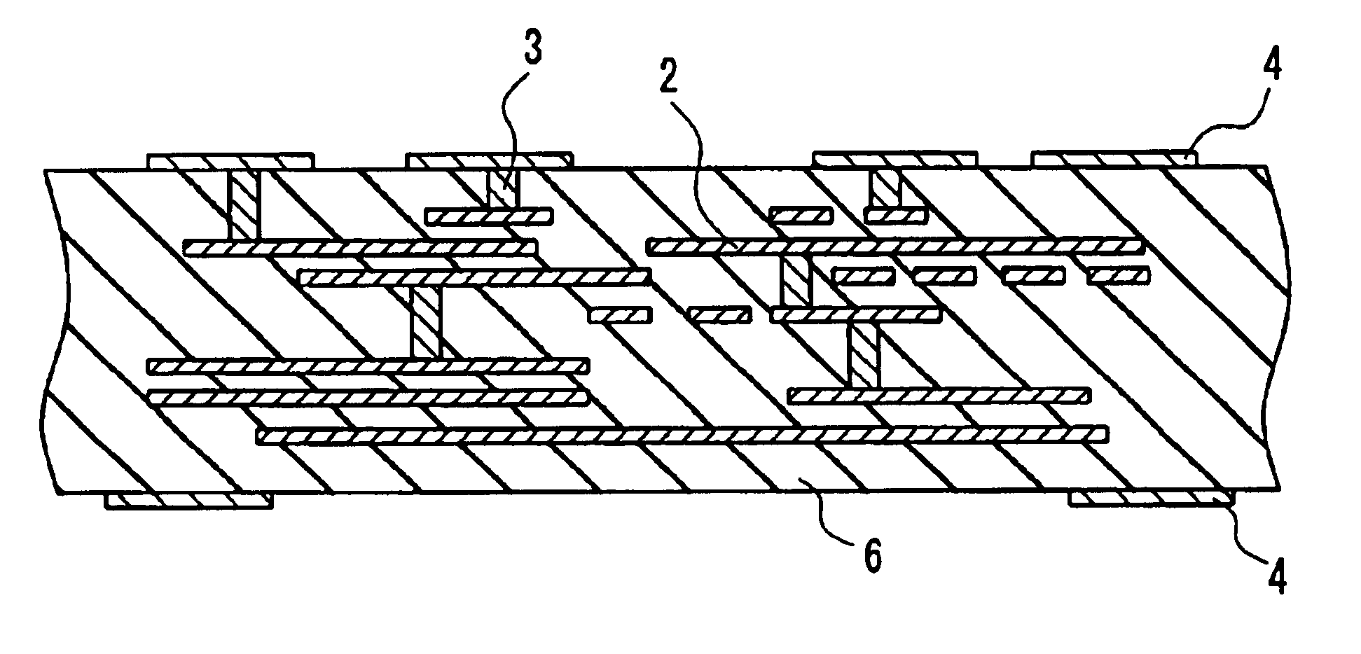
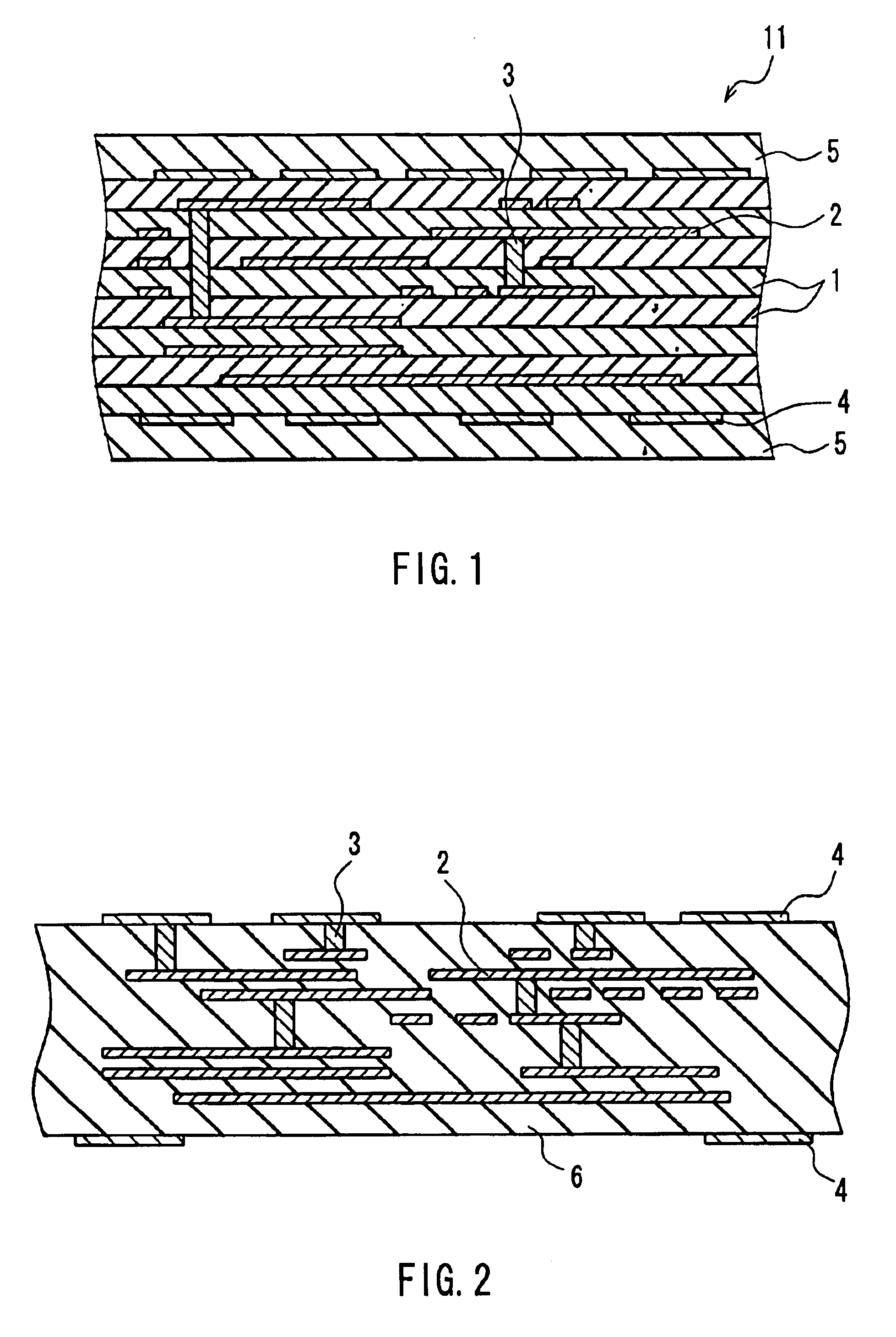
Multilayer ceramic substrate and method for manufacturing the same
a multi-layer ceramic and substrate technology, applied in the field of multi-layer ceramic substrates, can solve the problems of difficult to produce a large flat substrate, and difficult to produce a substrate with high dimensional accuracy
- Summary
- Abstract
- Description
- Claims
- Application Information
AI Technical Summary
Benefits of technology
Problems solved by technology
Method used
Image

Examples
example 1
A multilayer ceramic substrate of the above embodiment was produced and evaluated with actual measurement. In this example, the multilayer ceramic substrates were produced by using conductor compositions that differ in conductive powder or Mo compound, and then the electrode and the ceramic body of each of the multilayer ceramic substrates were evaluated. Table 1 shows the results. The conductor compositions in Example 1 did not include a glass frit.
The multilayer ceramic substrates were evaluated based on the conductor resistance of an electrode and defects or cracks caused at the interface between a via electrode and a ceramic body or in the vicinity thereof. For defects caused in the vicinity of the via electrode, the cross section of the fired substrate was polished and observed with a microscope.
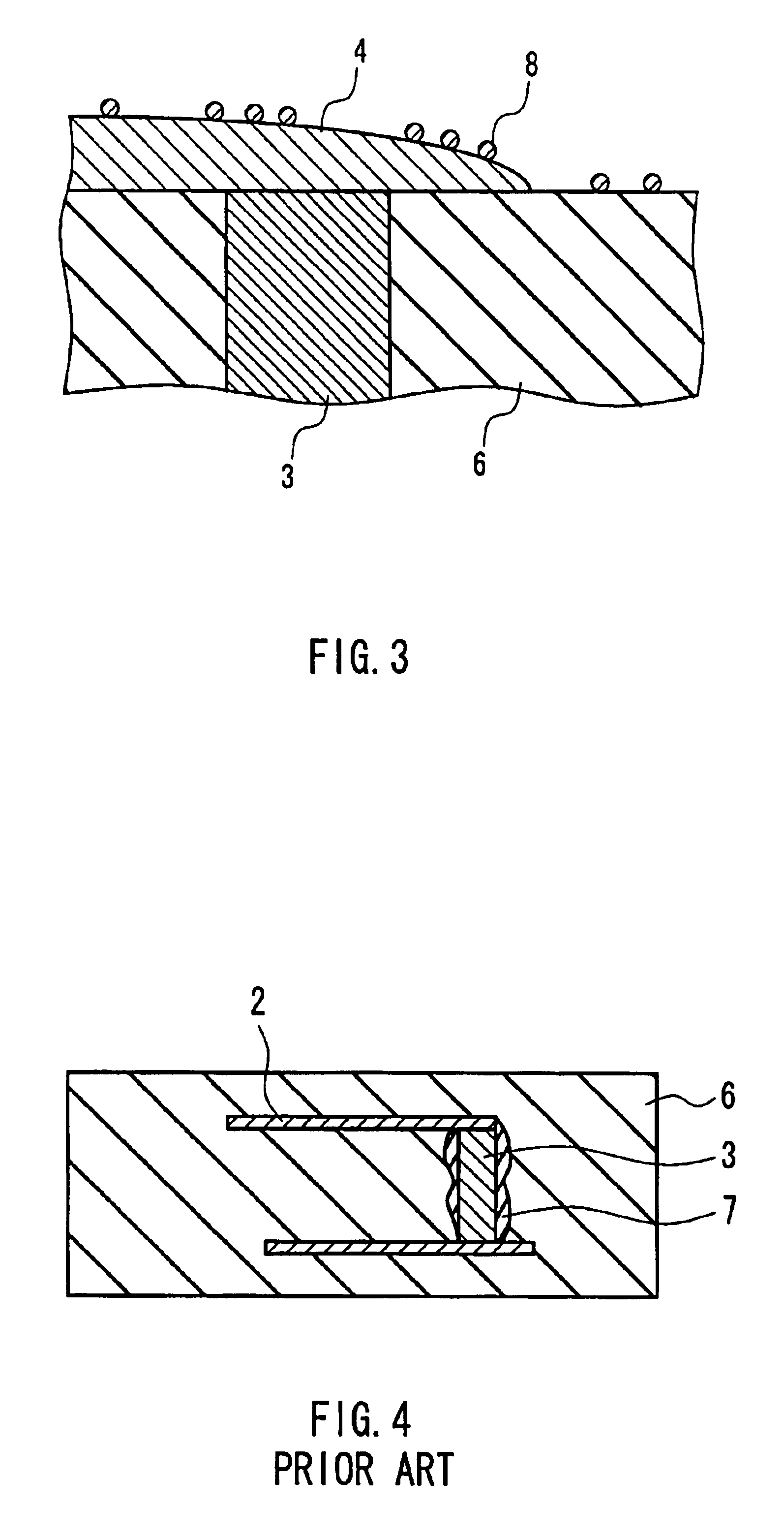
Table 1 shows as a comparative example the measurement of a multilayer ceramic substrate that was produced by using a conductor composition made of Ag powder alone. In this case, a defe...
example 2
Multilayer ceramic substrates were produced by using conductor compositions that differ in the softening point and the amount of a glass frit, and then the electrode and the ceramic body of each of the multilayer ceramic substrates were evaluated in the same manner as Example 1. Table 2 shows the results.
The conductor compositions of No. 17 and No. 18 included a glass frit with a softening point of less than 650.degree. C. The multilayer ceramic substrates using these conductor compositions had defects in the vicinity of the via electrode. The reason for this is considered to be as follows: the glass frit has a low softening point, and thus sintering of the conductive powder proceeds in the early stage, which leads to a difference in sintering timing between the conductive powder and the green sheet.
The conductor compositions of No. 19 to No. 21 included a glass frit with a softening point of not less than 650.degree. C. Therefore, no defect was caused in the vicinity of the via ele...
PUM
| Property | Measurement | Unit |
|---|---|---|
| softening point | aaaaa | aaaaa |
| thickness | aaaaa | aaaaa |
| particle diameter | aaaaa | aaaaa |
Abstract
Description
Claims
Application Information