MEMS structure with raised electrodes

a technology of raised electrodes and membranes, applied in the field of electrochemical components and structures, can solve the problems prone to drift of surface potentials on dielectric surfaces, repeatability of positioning, etc., and achieve the effect of mitigating the effect of uncontrollable dielectric surface potentials

Inactive Publication Date: 2004-09-14
GLIMMERGLASS NETWORKS
View PDF8 Cites 15 Cited by
  • Summary
  • Abstract
  • Description
  • Claims
  • Application Information

AI Technical Summary

Benefits of technology

According to the invention, in an electrostatically controlled deflection apparatus, such as a MEMS array having cavities formed around electrodes and which is mounted directly on a dielectric or controllably resistive substrate in which are embedded electrostatic actuation electrodes disposed in alignment with the individual MEMS elements, a mechanism is provided to mitigate the effects of uncontrolled dielectric surface potentials between the MEMS elements and the electrostatic actuation electrodes, the mechanism being raised electrodes relative to the dielectric or controllably resistive surface of the substrate. The aspect ratio of the gaps between elements (element height to element separation ratio) is at least 0.1 and preferably at least 0.5 and preferably between 0.75 and 2.0 with a typical choice of about 1.0, assuming a surface fill factor of 50% or greater. Higher aspect ratios at these fill factors provide incremental marginal improvement.

Problems solved by technology

One of the problems encountered is control of the surface potentials between the electrodes and control of the surface potentials on the insulators.
Surface potentials on dielectric surfaces are prone to drift over time due to charge migration along dielectric surfaces between said electrodes.
This can cause serious problems regarding repeatability of positioning.
An issue that arises is that the potential of these surfaces is not controlled due to non-linear conduction across the surfaces of ions and charges that accumulate in an uncontrolled fashion.
The conduction characteristics of these surfaces are inherently unstable due to sensitivity to temperature, moisture and other environmental factors.
They can also be affected by electromagnetic radiation (light), which can be time dependent depending on the application, contributing to system crosstalk.
The conductivity of these surfaces is also strongly affected by impurities and process steps and materials used in the deposition and etching of the surfaces.
All of these factors combined contribute to a loss of control of the surface potentials that contribute to the forces and torques applied to the actuatable elements resulting in an unreliable and uncontrollable device.

Method used


Image

  • MEMS structure with raised electrodes
  • MEMS structure with raised electrodes
  • MEMS structure with raised electrodes

Examples


Embodiment Construction

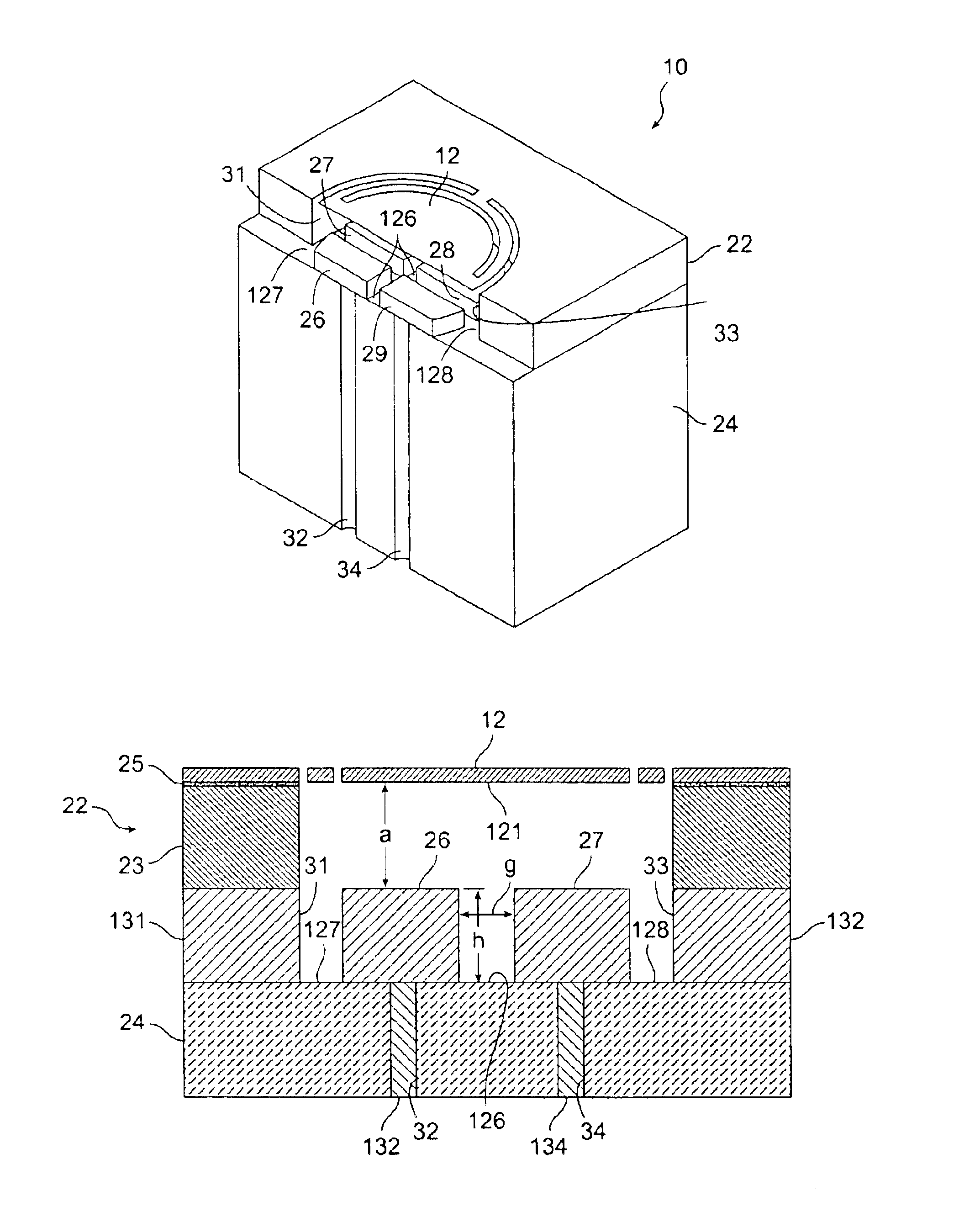
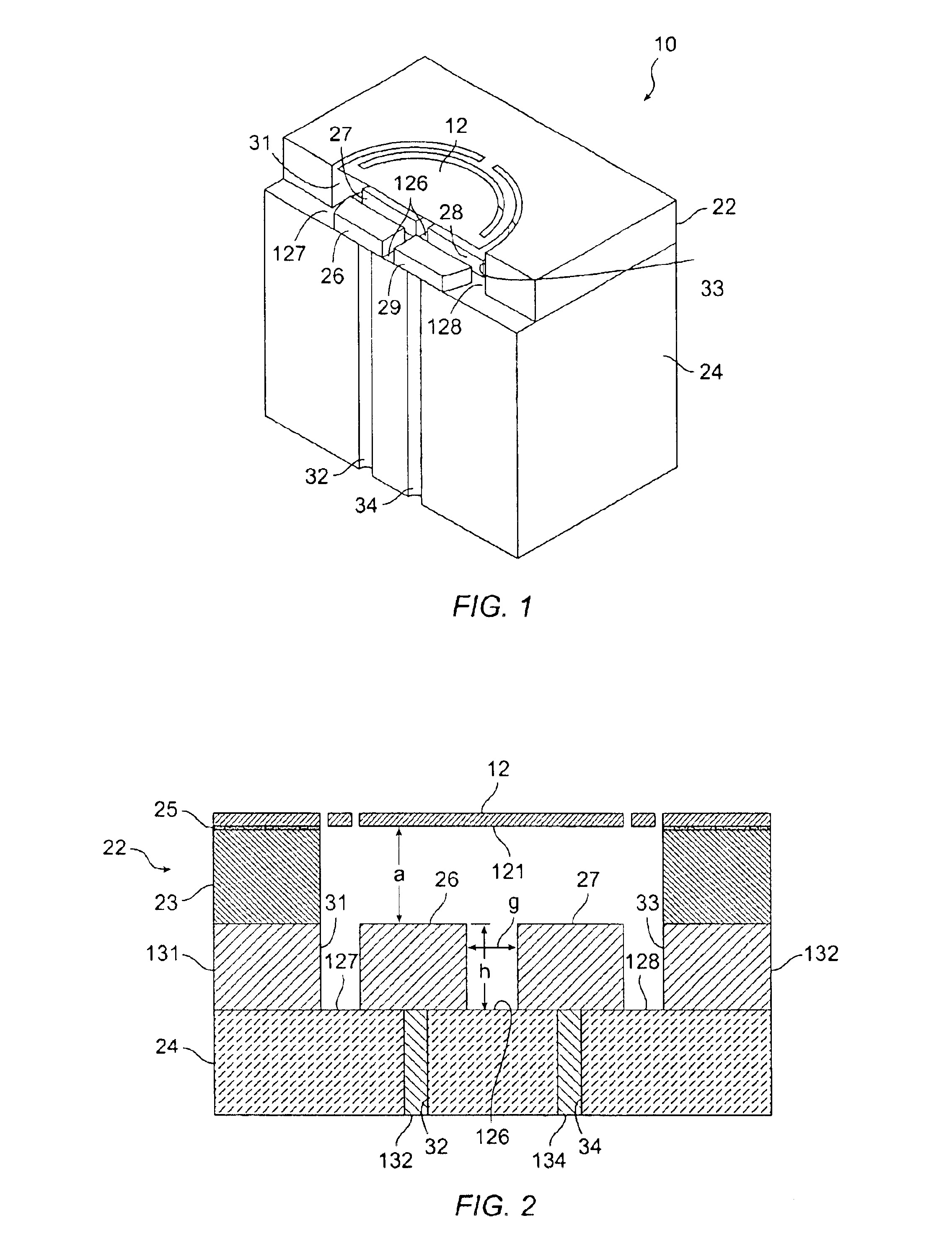
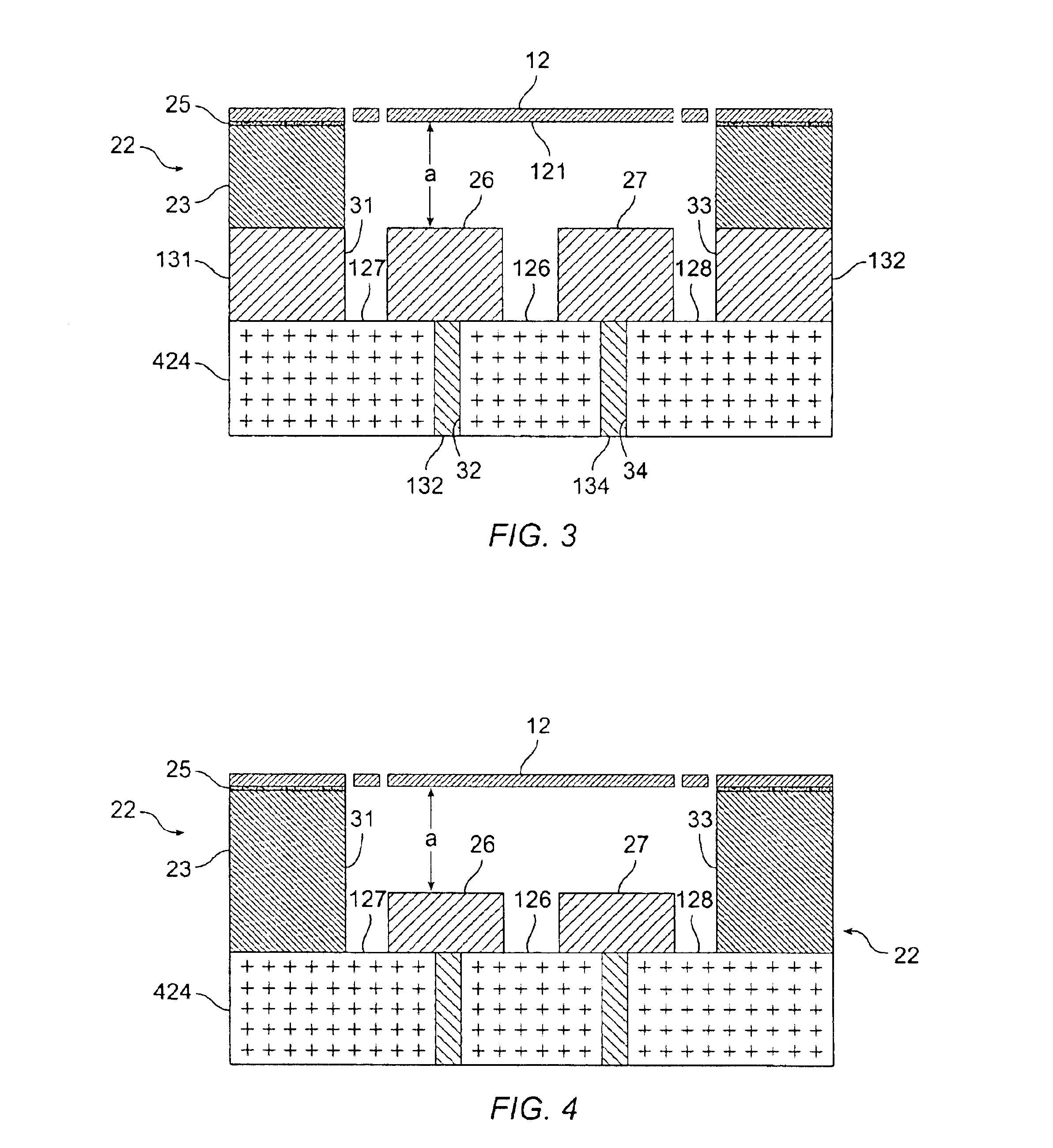
Reference is made to FIG. 1 in which is shown a single MEMS (Micro Electro-Mechanical Systems) array element 10 according to the invention, with a MEMS-based mirror 12 fabricated in an integrated Silicon on Insulator (SOI) structure (a MEMS structure) 22 and mounted on a substrate or base 24, which is typically electrically insulative. According to the invention, and referring also to FIG. 2, a mechanism is provided whereby the effects of uncontrolled surface potentials are mitigated through use of raised electrodes 26-29 and optionally highly resistive interstitial regions 126 between the several electrodes 26-29 and interstitial regions 127, 128 between the raised electrodes 26-29 and surrounding conductive sidewalls or surfaces 31 and 33. The electrodes 26-29 are connected to voltage sources (not shown) through vias 32, 34, etc. containing a conductive material, such as a metal 132, 134. The structure of element 10 shown in FIG. 1 is not specific to a particular configuration. Va...


PUM


Abstract

In an electrostatically controlled deflection apparatus, such as a MEMS array having cavities formed around electrodes and which is mounted directly on a dielectric or controllably resistive substrate in which are embedded electrostatic actuation electrodes disposed in alignment with the individual MEMS elements, a mechanism is provided to mitigate the effects of uncontrolled dielectric surface potentials between the MEMS elements and the electrostatic actuation electrodes, the mechanism being raised electrodes relative to the dielectric or controllably resistive surface of the substrate. The aspect ratio of the gaps between elements (element height to element separation ratio) is at least 0.1 and preferably at least 0.5 and preferably between 0.75 and 2.0 with a typical choice of about 1.0, assuming a surface fill factor of 50% or greater. Higher aspect ratios at these fill factors are believed not to provide more than marginal improvement.

Description

STATEMENT AS TO RIGHTS TO INVENTIONS MADE UNDER FEDERALLY SPONSORED RESEARCH OR DEVELOPMENTNOT APPLICABLEBACKGROUND OF THE INVENTIONThis invention relates to electro ceramic components and structures that accurately control surface potentials around electro ceramic components. Components constructed according to the invention can be Micro Electro Mechanical System (MEMS) devices, MEMS arrays, or other micromachined elements.Conventional MEMS array structures comprise Silicon on Insulator (SOI) array structures associated with an electrode array disposed to interact with the MEMS actuatable elements. Electrostatic MEMS structures develop forces and torques between the actuatable elements and their corresponding electrodes. Conventional MEMS structures separate conductive surfaces with dielectrics. These dielectrics contribute to the mechanical operation of the device because accumulated charge distributions on their surfaces contribute to the electrostatic force and / or torque on the ...

Claims


Application Information

Patent Timeline
Patent Type & Authority Patents(United States)
IPC IPC(8): B81B3/00G02B26/08
CPCB81B3/0086G02B26/0841B81B2201/042
Inventor STAKER, BRYAN P.MURAY, LAWRENCE P.FERNANDEZ, ANDRES
Owner GLIMMERGLASS NETWORKS
Why Eureka
Try Eureka