Scaled EEPROM cell by metal-insulator-metal (MIM) coupling

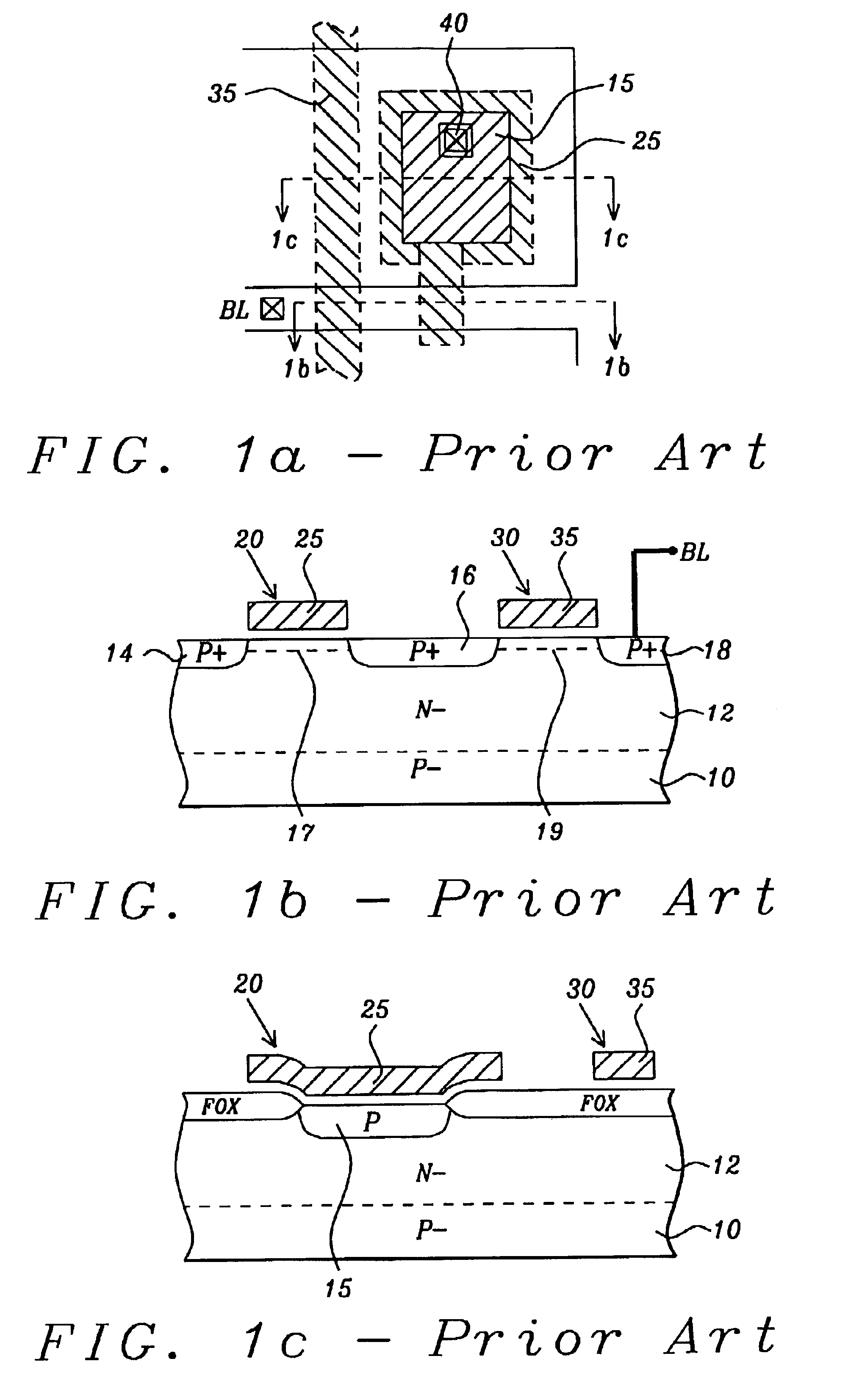
a technology of metal-insulator metal and coupling capacitor, which is applied in the direction of capacitors, transistors, solid-state devices, etc., can solve the problems of limiting the extent to which the size of such cells may be reduced, and the buried junction of control gate (15) of fig. 1c normally experiences breakdown, so as to achieve the effect of reducing the cell area

Inactive Publication Date: 2004-11-16
TAIWAN SEMICON MFG CO LTD
View PDF7 Cites 26 Cited by
  • Summary
  • Abstract
  • Description
  • Claims
  • Application Information

AI Technical Summary

Benefits of technology

It is therefore an object of the present invention to provide a single-poly EEPROM device having a verti

Problems solved by technology

These high programming and erase voltages limit the extent to which the size of such cells may be reduced.
However,

Method used


Image

  • Scaled EEPROM cell by metal-insulator-metal (MIM) coupling
  • Scaled EEPROM cell by metal-insulator-metal (MIM) coupling
  • Scaled EEPROM cell by metal-insulator-metal (MIM) coupling

Examples


Embodiment Construction

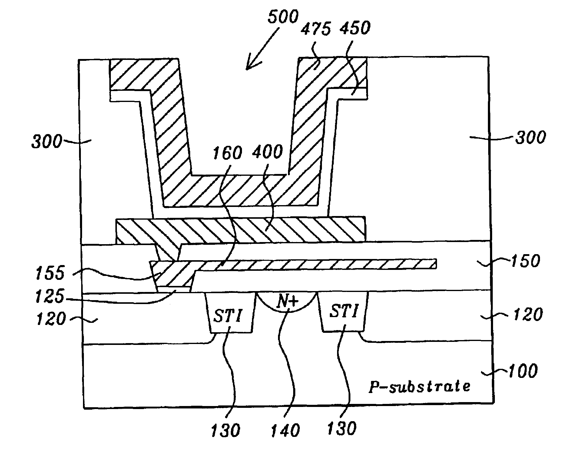
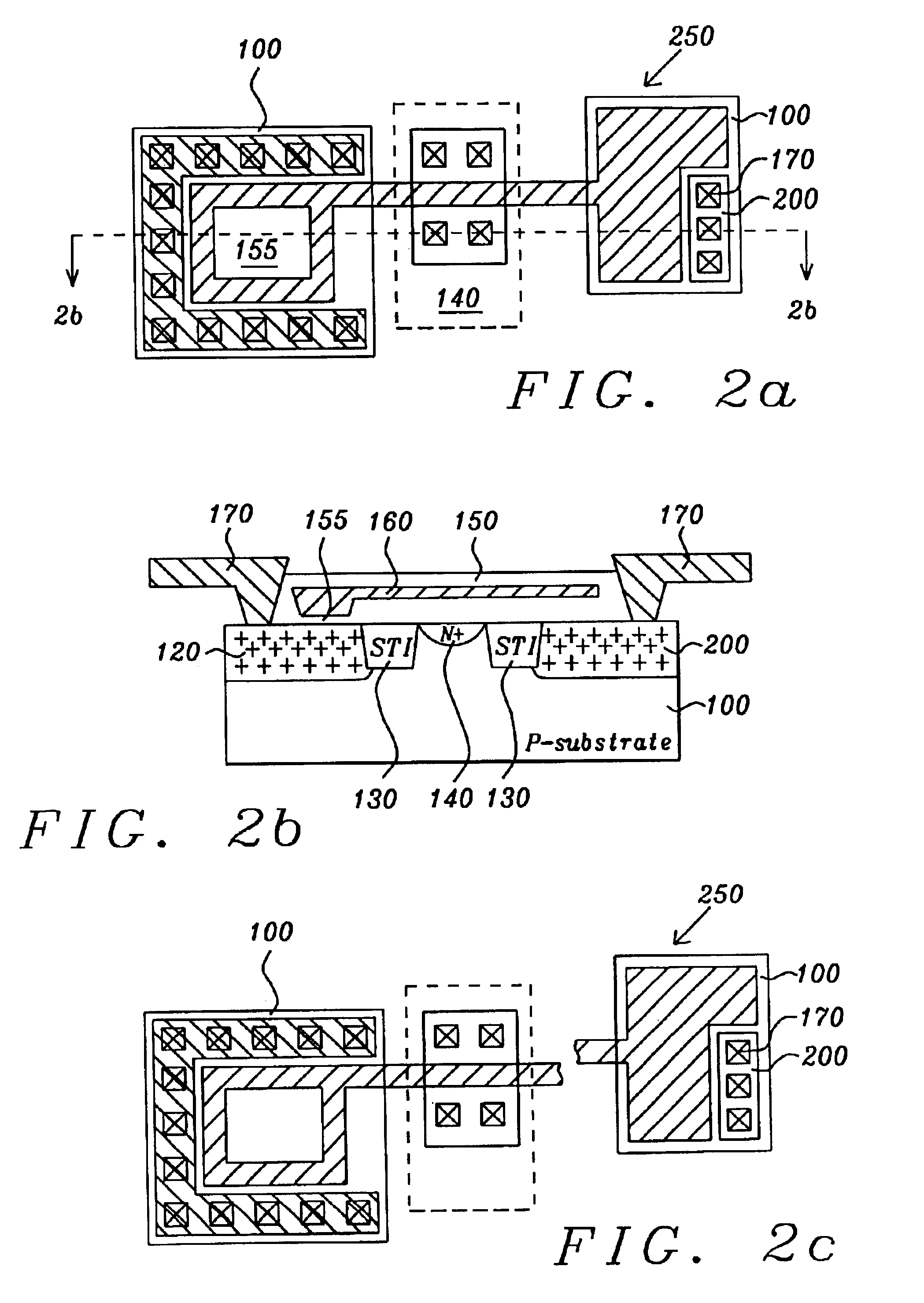
Referring now to the drawings, FIGS. 2a-2c show a single-poly EEPROM cell with a buried lateral control gate as practiced in the current manufacturing line. On the other hand, FIGS. 3a-3c disclose how the state of the art single-poly cell of FIGS. 2a-2c can be converted to a device having a vertically formed metal-insulator-metal (MIM) capacitor, which serves as a control gate in place of the buried control gate, thus scaling down the size of the cell by more than 25%. Furthermore, in the absence of the buried control gate, the well-known junction breakdown issue is eliminated, and at the same time, other known benefits such as increased coupling ratio of the control gate as well as low erase voltage are realized. FIGS. 4a-4h describe a method of forming the disclosed MIM capacitor and the cell thereof.

In FIG. 2a, a top view of the substrate in FIG. 2b is shown. FIG. 2b is a cross-sectional view taken at 2b-2b shown in FIG. 2a. Numeral (100) references a partial cross section of a s...


PUM


Abstract

A single-poly EEPROM cell is disclosed with a vertically formed metal-insulator-metal (MIM) coupling capacitor, which serves as a control gate in place of a laterally buried control gate thereby eliminating the problem of junction breakdown, and at the same time reducing the size of the cell substantially. A method of forming the single-poly cell is also disclosed. This is accomplished by forming a floating gate over a substrate with an intervening tunnel oxide and then the MIM capacitor over the floating gate with another intervening dielectric layer between the top metal and the lower metal of the capacitor where the latter metal is connected to the polysilicon floating gate.

Description

BACKGROUND OF THE INVENTION(1) Field of the InventionThe present invention relates to semiconductor manufacturing and is more particularly directed to a single-poly EEPROM (electrically erasable programmable read only memory) cell formed with a MIM (Metal-Insulator-Metal) coupling capacitor, and also to a method of forming the same.(2) Description of the Related ArtIt is the preferred practice in the art that, when embedding memory cells into a standard logic process, the single-poly process that is typically used in the fabrication of logic circuitry not be altered. This has led to the development of a single-poly EEPROM cell having N+ source and N+ drain regions formed in a P-substrate and a polysilicon gate overlying a channel region extending between the source and the drain. An N diffusion region formed in the P-substrate serves as the control gate and is capacitevely coupled to the floating gate via a thin oxide layer. The oxide layer has a tunnel window opened in a portion th...

Claims


Application Information

Patent Timeline
IPC IPC(8): H01L21/02H01L29/423H01L21/336H01L21/28H01L29/40
CPCH01L21/28273H01L28/40H01L29/66825H01L29/42324H01L28/91H01L29/40114
Inventor LIN, CHRONG JUNCHEN, HSIN-MING
Owner TAIWAN SEMICON MFG CO LTD
Why Eureka
Try Eureka