Multimode data buffer and method for controlling propagation delay time

a data buffer and multi-mode technology, applied in the field of multi-mode data buffers and a control method of propagation delay time, can solve the problems of limiting the bandwidth between the synchronous dram and the dram controller, the data input/output of the memory device in a unit time is limited, and the data setup/hold time margin may be degraded

Inactive Publication Date: 2004-11-16
SAMSUNG ELECTRONICS CO LTD
View PDF11 Cites 99 Cited by
  • Summary
  • Abstract
  • Description
  • Claims
  • Application Information

AI Technical Summary

Problems solved by technology

However, since a data input / output operation in a synchronous DRAM should be performed in a cycle of a system clock, there is a limit to increasing the bandwidth between the synchronous DRAM and a DRAM controller, that is, the amount of data which is input / output from a memory device in a unit time is limited.
However, in a DDR synchronous DRAM having an SM-type data strobe signal input buffer, a data setup / hold time margin may be degraded if noise is included in a data strobe signal or reference voltage.
However, since the gain of a differential amplifier in the single mode is different from the gain in the dual mode, the propagation delay time in the single mode is different from the propagation delay time in the dual mode.
The difference in the propagation delay time may cause a difference in the setup / hold timing in each mode such that a data setup / hold margin is degraded.

Method used


Image

  • Multimode data buffer and method for controlling propagation delay time
  • Multimode data buffer and method for controlling propagation delay time
  • Multimode data buffer and method for controlling propagation delay time

Examples


Embodiment Construction

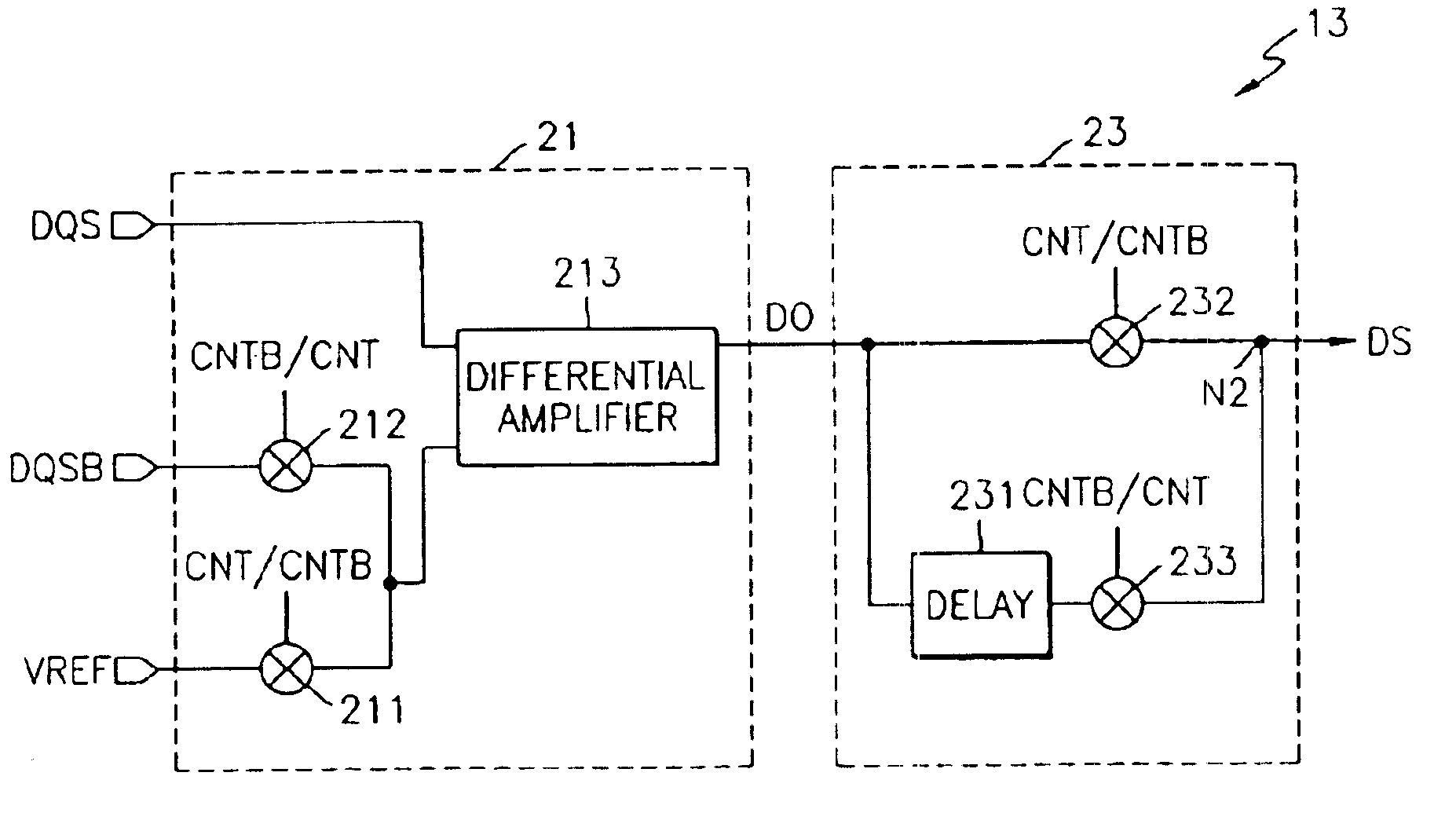
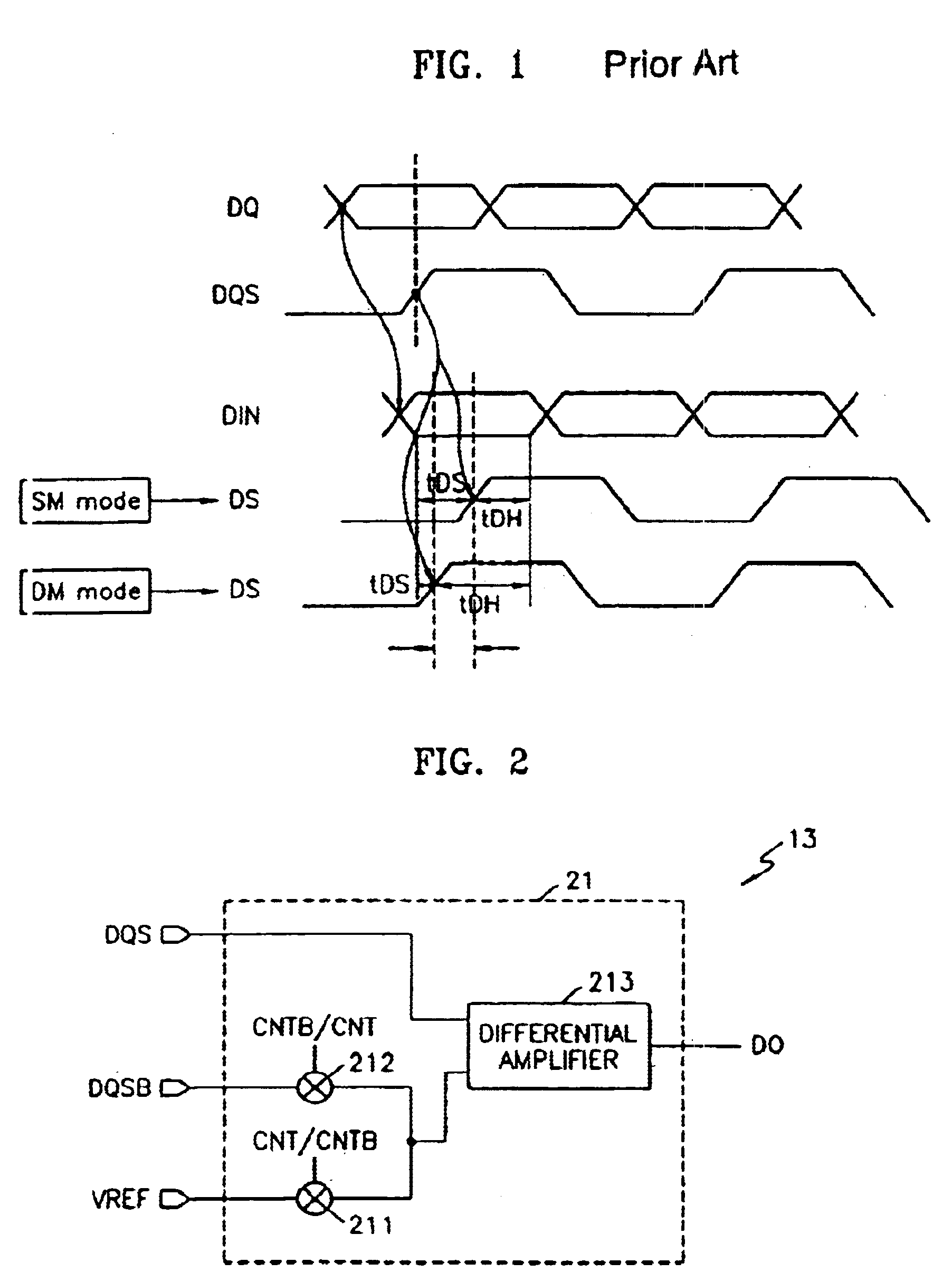
FIG. 2 is a block diagram of a data strobe input buffer according to an exemplary embodiment of the present invention. The data strobe input buffer 13 is a multimode data strobe input buffer, for example, a single mode / dual mode (SM / DM) double-use data strobe input buffer. In response to a control signal (CNT / CNTB), the data strobe input buffer 13 differentially amplifies a data strobe signal (DQS) and a reference voltage (VREF), or the data strobe signal (DQS) and an inverse data strobe signal (DQSB).

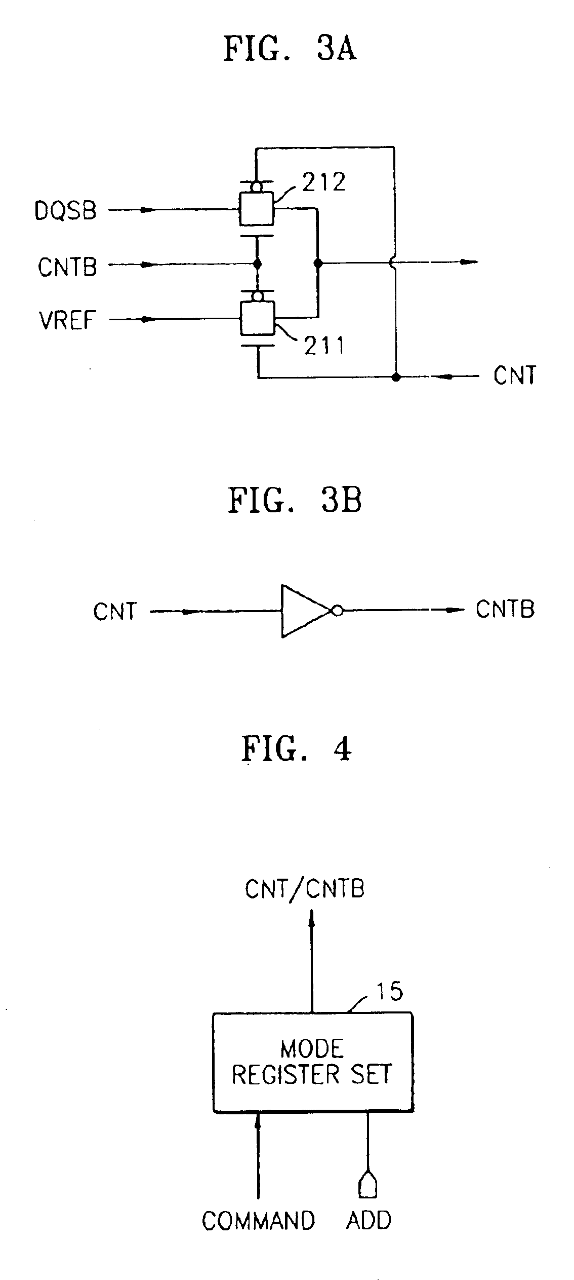
More specifically, the data strobe input buffer 13 includes a differential amplification circuit 21. The differential amplification circuit 21 further includes one or more switches 211 and 212, and a differential amplifier 213. In an exemplary embodiment, the switches 211 and 212 are formed as transmission gates.

If the control signal (CNT) is at a first logic state, for example, in a "high" logic level, the switch 211 is turned on and the switch 212 is turned off. Accordingly, the diff...


PUM


Abstract

A data buffer, such as a data strobe input buffer or a data input buffer, which may operate in multiple modes, such as a single mode (SM) and a dual mode (DM) and where the mode is selected by providing a signal, such as an external signal such as an address signal or an external command signal. A data buffer which can be used for a SM / DM dual-use and can improve a data setup / hold margin. A semiconductor memory device including one or more of the data buffers described above. A method for controlling propagation delay times which can improve a data setup / hold margin in a SM / DM dual-use data buffer.

Description

1. Field of the InventionThe present invention relates to a semiconductor memory device, and more particularly, to a multimode data buffer and a method for controlling propagation time delay.2. Description of the Related ArtTo improve system performances, innovations in the design of semiconductor memory devices in general, and the design of dynamic random access memories (DRAMs) in particular, continue to focus on higher integration and higher speed operation. That is, DRAMs capable of processing more data at higher speed are desired. For higher speed operations, DRAMs synchronized with a system clock have been developed. This synchronous feature of DRAMs has increased data transmission speeds.However, since a data input / output operation in a synchronous DRAM should be performed in a cycle of a system clock, there is a limit to increasing the bandwidth between the synchronous DRAM and a DRAM controller, that is, the amount of data which is input / output from a memory device in a uni...

Claims


Application Information

Patent Timeline
Patent Type & Authority Patents(United States)
IPC IPC(8): G11C7/10G11C11/409G11C11/407
CPCG11C7/1045G11C7/109G11C7/1084G11C7/1078G11C7/10
Inventor SEO, SEONG-YOUNGLEE, JUNG-BAEMOON, BYONG-MO
Owner SAMSUNG ELECTRONICS CO LTD
Why Eureka
Try Eureka