Method for fabricating a mask read-only-memory with diode cells

a diode cell and read-only memory technology, applied in the field of mask rom fabrication, can solve the problems of code pattern resolution enhancement and inability to well define the code ion implanted region

Inactive Publication Date: 2004-11-23
MACRONIX INT CO LTD
View PDF1 Cites 14 Cited by
  • Summary
  • Abstract
  • Description
  • Claims
  • Application Information

AI Technical Summary

Problems solved by technology

However, when the mask ROM device is shrunk down, the issue of the code pattern resolution is enhanced and the code ion implanted region cannot be well defined.

Method used


Image

  • Method for fabricating a mask read-only-memory with diode cells
  • Method for fabricating a mask read-only-memory with diode cells
  • Method for fabricating a mask read-only-memory with diode cells

Examples


Embodiment Construction

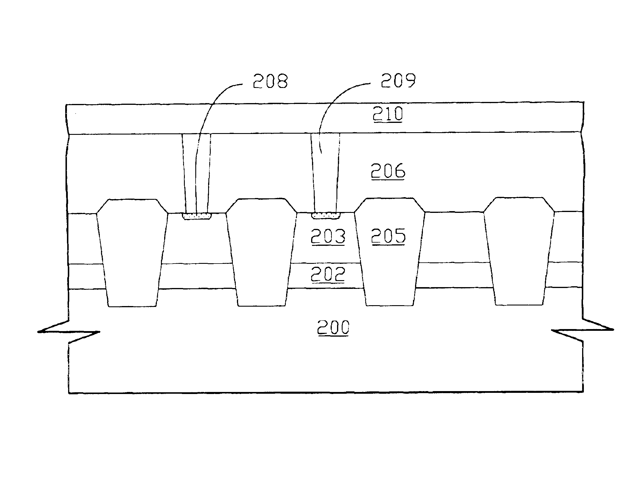
The present invention provides a method for fabricating a mask ROM with diode cells, which uses a structure of a contact plug / a PN diode instead of a channel transistor to serve as a memory cell. The process for forming the structure of the contact plug / PN diode is simple and can provide a well-defined code area even though the device dimension is shrunk down. The manufacturing cost is also reduced. Furthermore, the area of the semiconductor substrate occupied by one PN diode is smaller than that of the channel transistor. Thus, a high-density mask ROM device can be obtained by the present method.

The present method for fabricating a mask ROM with diode cells will be described in detail according to one preferred embodiment of the present invention with reference to the accompanying drawings.

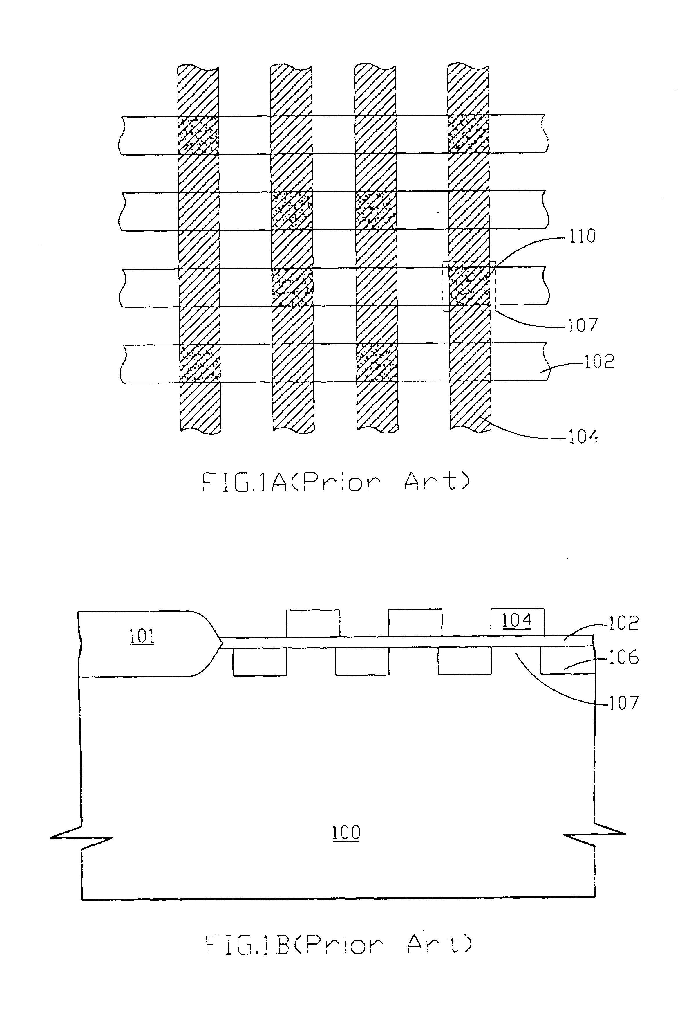
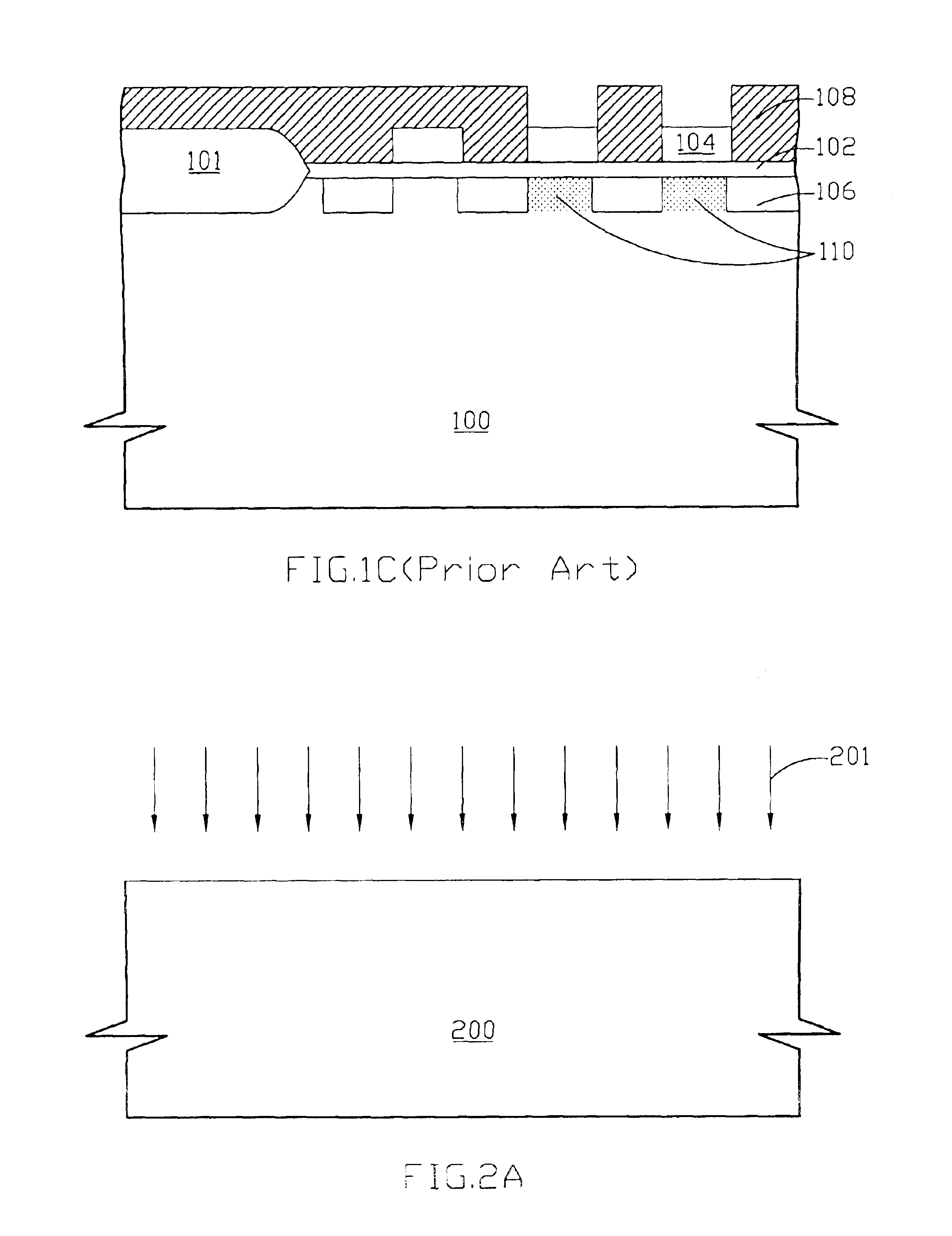
FIGS. 2A to 2E are schematic cross-sectional views of various steps for fabricating a mask ROM with diode cells according to one preferred embodiment of the present invention. Firstly, referring ...


PUM


Abstract

A method for fabricating a mask read-only-memory with diode cells is provided. A doped conductive layer with a first conductivity is formed on bit lines. Then, a photoresist layer with a mask ROM pattern is formed on an interlayer dielectric layer on the doped conductive layer for serving as an etching mask, thereby forming openings in the interlayer dielectric layer unto the exposed regions of the doped conductive layer. Performing ion implantation to form a diffusion region with a second conductivity opposite to the first conductivity in each exposed region of the doped conductive layer, so that the doped conductive layer and the diffusion regions formed therein constitute diode cells that are served as memory cells. A contact plug is formed in each opening unto the diode cell and a conductive layer is formed on the contact plug for serving as word lines.

Description

1. Field of the InventionThe present invention relates to a method for fabricating a mask read-only-memory (mask ROM), and more particularly to a method for fabricating a mask ROM with diode cells.2. Description of the Prior ArtMemory cells of a mask ROM (mask read-only-memory) are is generally made using channel transistors. Programming of the ROM is achieved by selectively implanting ions into the channels of these transistors. By implanting ions into the channel regions of specified transistors, threshold voltage of the devices changes. Hence, the "on" or "off " state of the memory cell is coded. A mask ROM cell is formed by laying a polysilicon word line (WL) over a bit line (BL), and the memory cell channel is formed in the region underneath the word line between neighboring bit lines. Normally, each ROM cell is in a logic state of "1" or "0" depending on whether ions are implanted into the channel region or not. The advantage of being able to program the state of each ROM cell...

Claims


Application Information

Patent Timeline
Patent Type & Authority Patents(United States)
IPC IPC(8): H01L21/70H01L21/8242H01L21/8246H01L27/112
CPCH01L27/112H01L27/11253H01L27/1126H10B20/00H10B20/38H10B20/383
Inventor WU, CHUN-PEICHEN, HUEI-HUARNGTSAI, WEN-BINKAO, HSUAN-LING
Owner MACRONIX INT CO LTD
Why Eureka
Try Eureka