Power MOS transistor for absorbing surge current

a technology of surge current and power mos, which is applied in the direction of semiconductor devices, semiconductor/solid-state device details, electrical apparatus, etc., can solve the problems of unobtainable high breakdown voltage (characteristic bearing a high voltage), inability to achieve high breakdown voltage and low resistance as described before, and inability to meet high breakdown voltage and low resistan

Inactive Publication Date: 2004-12-14
DENSO CORP
View PDF51 Cites 41 Cited by
  • Summary
  • Abstract
  • Description
  • Claims
  • Application Information

AI Technical Summary

Problems solved by technology

In the case of such an LDMOS, if the concentration of the N well 2 is heightened in order to reduce the ON resistance to facilitate the current flow, difficulty is encountered to enlarge the depletion layer in the drift region, so that a high breakdown voltage (characteristic bearing a high voltage) becomes unobtainable.
Because of the occurrence of the large current passing through the narrow area, the elements are easy to heat so that the breakdown of the elements takes place irrespective of a low reverse voltage, thus resulting in impairing the breakdown proof of the elements.
In this case, although, if having the structure as shown in FIG. 50, the LDMOS, together with the NPNTr, can be formed on the same substrate, the compatibility of a high breakdown voltage and a low ON resistance as described before become impossible.
However, in the case that the load is driven by a high side switch type in which as shown in FIG. 10B the LDMOS is connected to the power supply side and the load is coupled to the GND side, in response to the switching of the LDMOS, the source electric potential greatly varies, which can also cause the switching noises.
However, in the case of the load driving element such as the LDMOS, the element size increase, thus creating such a problem.

Method used


Image

  • Power MOS transistor for absorbing surge current
  • Power MOS transistor for absorbing surge current
  • Power MOS transistor for absorbing surge current

Examples


first embodiment

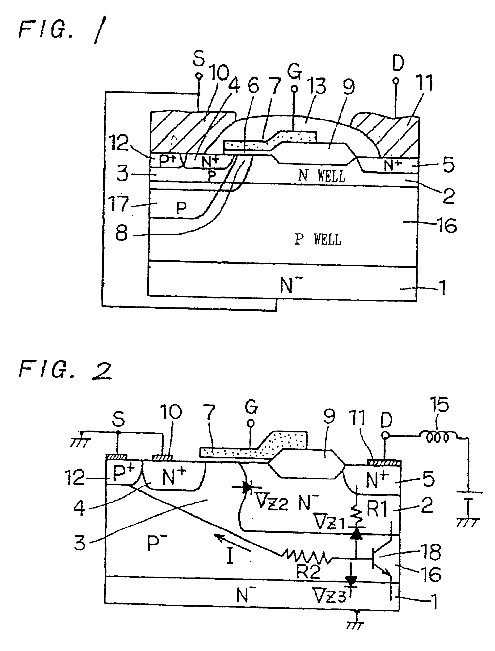
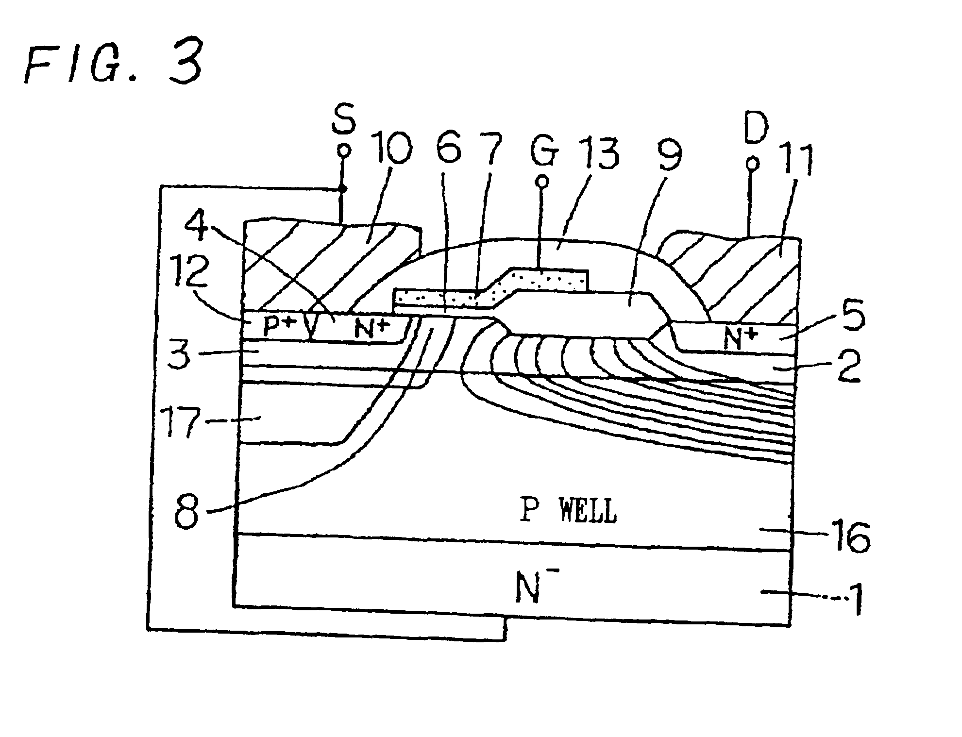
FIG. 1 is a cross-sectional view showing a structure of a reduced surface field strength type LDMOS according to the present invention. In this embodiment, as shown in FIG. 1 a P well 16 is disposed on an N-type Substrate and an N well 2 is formed in the P well 16 to thereby produce a double-well structure, with a source electrode 10 and the N-type substrate 1 being made to be equal in electric potential to each other. In a drift region of the N well 2, the dopant concentration is set to satisfy the so-called RESURF condition. Further, In the illustration, parts marked with the same reference numerals as those in FIGS. 8 and 9 have the same or corresponding structures.

The reduced surface field strength type LDMOS as shown in FIG. 1 has a high breakdown voltage and a low ON resistance and can prevent the breakdown of the channel formation portions at the time of the application of a reverse voltage occurring when an L load comes into connection with a drain electrode, as will be desc...

second embodiment

Moreover, a description will be made hereinbelow of a concrete structure of a reduced surface field strength type LDMOS formed in an insulated and separated element region according to the present invention. FIG. 8 is a cross-sectional view showing the structure of the reduced surface field strength type LDMOS according to this embodiment, where the portion other than a deep N.sup.+ diffused layer 126 d N.sup.+ substrate 121b corresponds to the reduced surface field strength type LDMOS showing in FIG. 1. The elements 103-107 and 109-112 in FIG. 8 respectively correspond to elements 3-7 and 9-12 in FIGS. 1-3. In the FIG. 8 structure, a P well 129 and a base 130 are provided in order to fix the electric potential of a P well 116 to the source electric potential. FIG. 9 is a plan view showing the structure shown in FIG.8. In an element region separated and formed by an oxide film 123 to have an island-like configuration, there is provided a cell region 31 in which a plurality of LDMOS ...

third embodiment

Referring now to FIG. 14, a description will be made hereinbelow of the present invention.

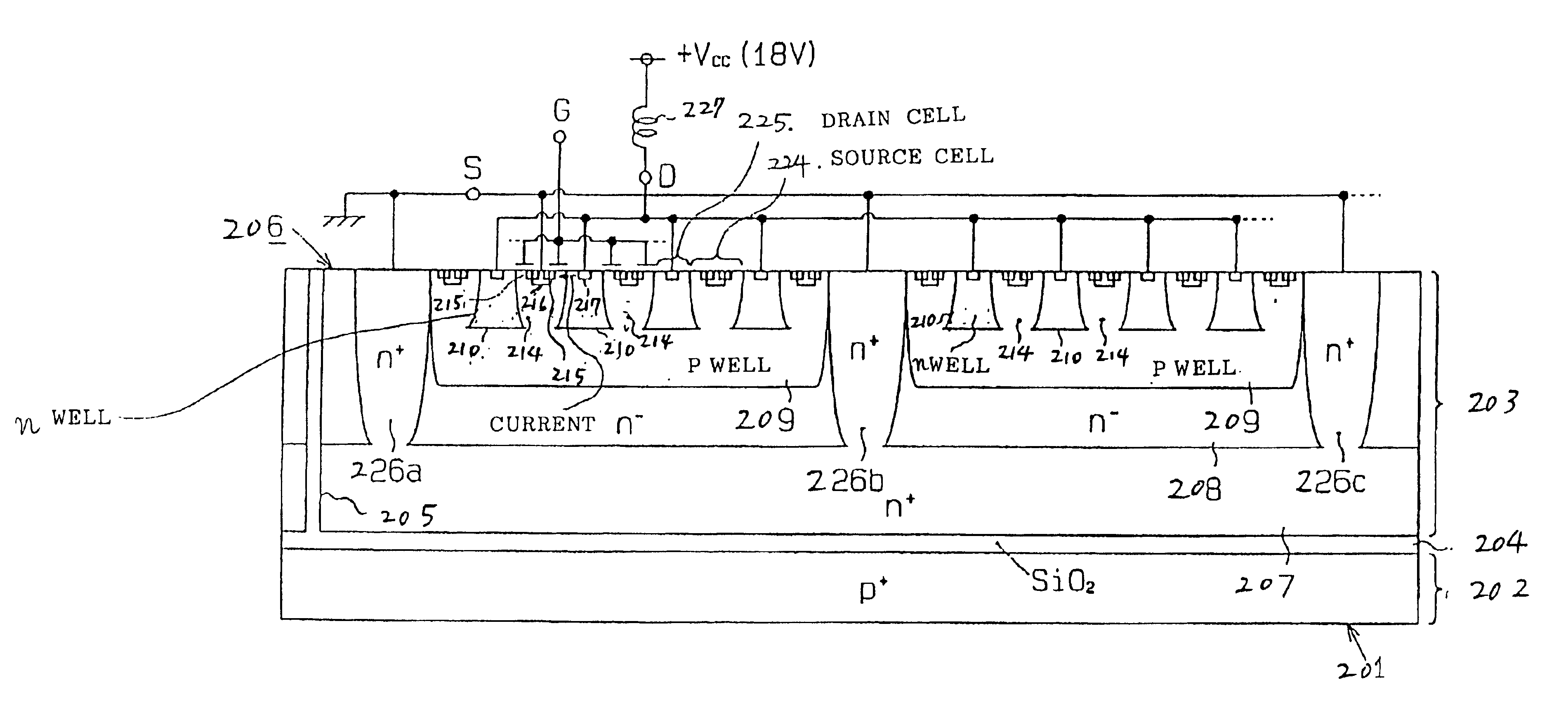
FIG. 14 is a plan view showing a structure of power MOS transistor according to this embodiment and FIG. 15 is a cross-sectional view taken along a line II--II of FIG. 14, that is, shows a cross section of a silicon chip 201 serving as semiconductor substrate. In this embodiment, islands are produced and defined through an SOI (Silicon On Insulator) structure and a separation structure based on a trench oxide film. Formed within an island is a lateral power MOS transistor which is the n-channel type. Incidentally, a device incorporating this transistor is applicable to a controller for motor vehicles and a battery (18V) mounted on a motor vehicle is used as a power supply therefor.

In FIG. 15, a p.sup.+ silicon substrate 202 and an n-type silicon substrate 203 are joined with each other by lamination in a state where a silicon oxide film (buried oxide film) 204 is interposed therebetween, thus p...


PUM


Abstract

A semiconductor device is provided having a power transistor structure. The power transistor structure includes a plurality of first wells disposed independently at a surface portion of a semiconductor layer; a deep region having a portion disposed in the semiconductor layer between the first wells; a drain electrode connected to respective drain regions in the first wells; a source electrode connected to respective source regions and channel well regions in the first wells, such that either the drain electrode or the source electrode is connected to an inductive load; and a connecting member for supplying the deep region with a source potential, where the connecting member is configurable to connect to the drain electrode when the drain electrode is connected to the inductive load and to connect to the source electrode when the source electrode is connected to said inductive load.

Description

1. [Field of the Invention]The present invention relates to a semiconductor device with a reduced surface field strength type MOS transistor, a method of manufacturing the same semiconductor device, and a semiconductor device with a load driving semiconductor element such as an LDMOS (Lateral Diffused MOS) transistor (which will be referred hereinafter to as an LDMOS), and further an LDMOS (Lateral Double Diffused) transistor such as a power transistor serving as a large-current type switching element.2. [Description of the Prior Art]As an N-channel LDMOS there has been known an element with a structure as shown in FIG. 50. As illustrated, this LDMOS has an N-type substrate 1, an N well 2 deposited on the N-type substrate 1, a channel P well 3 formed in the N well 2, an N-type diffused layer 4 formed in the channel P well 3 and a different N-type diffused layer 5 provide in the N well 2. In addition, a gate electrode 7 is located on a substrate surface in a state that a gate oxide f...

Claims


Application Information

Patent Timeline
Patent Type & Authority Patents(United States)
IPC IPC(8): H01L29/66H01L21/70H01L21/02H01L29/78H01L21/336H01L29/739H01L21/8249H01L27/085H01L27/02H01L27/06H01L29/10
CPCH01L21/8249H01L27/0251H01L27/0623H01L27/085H01L29/7835H01L29/66674H01L29/7395H01L29/7801H01L29/7824H01L29/1087H01L29/7816
Inventor KITAMURA, YASUHIROSAKAKIBARA, TOSHIOKOHNO, KENJIMIZUNO, SHOJINAKAYAMA, YOSHIAKIMAEDA, HIROSHIIIDA, MAKIOFUJIMOTO, HIROSHISAITOU, MITSUHIROIMAI, HIROSHIBAN, HIROYUKI
Owner DENSO CORP
Why Eureka
Try Eureka