
Electromagnetic wave transforming device
a technology of transforming device and electromagnetic wave, which is applied in the direction of radioation control device, television system, instruments, etc., can solve the problems of deteriorating image quality adversely affecting image information, etc., and achieve accurate detecting of irradiation quantity
- Summary
- Abstract
- Description
- Claims
- Application Information
AI Technical Summary
Benefits of technology
Problems solved by technology
Method used
Image

Examples
first embodiment
(First Embodiment)
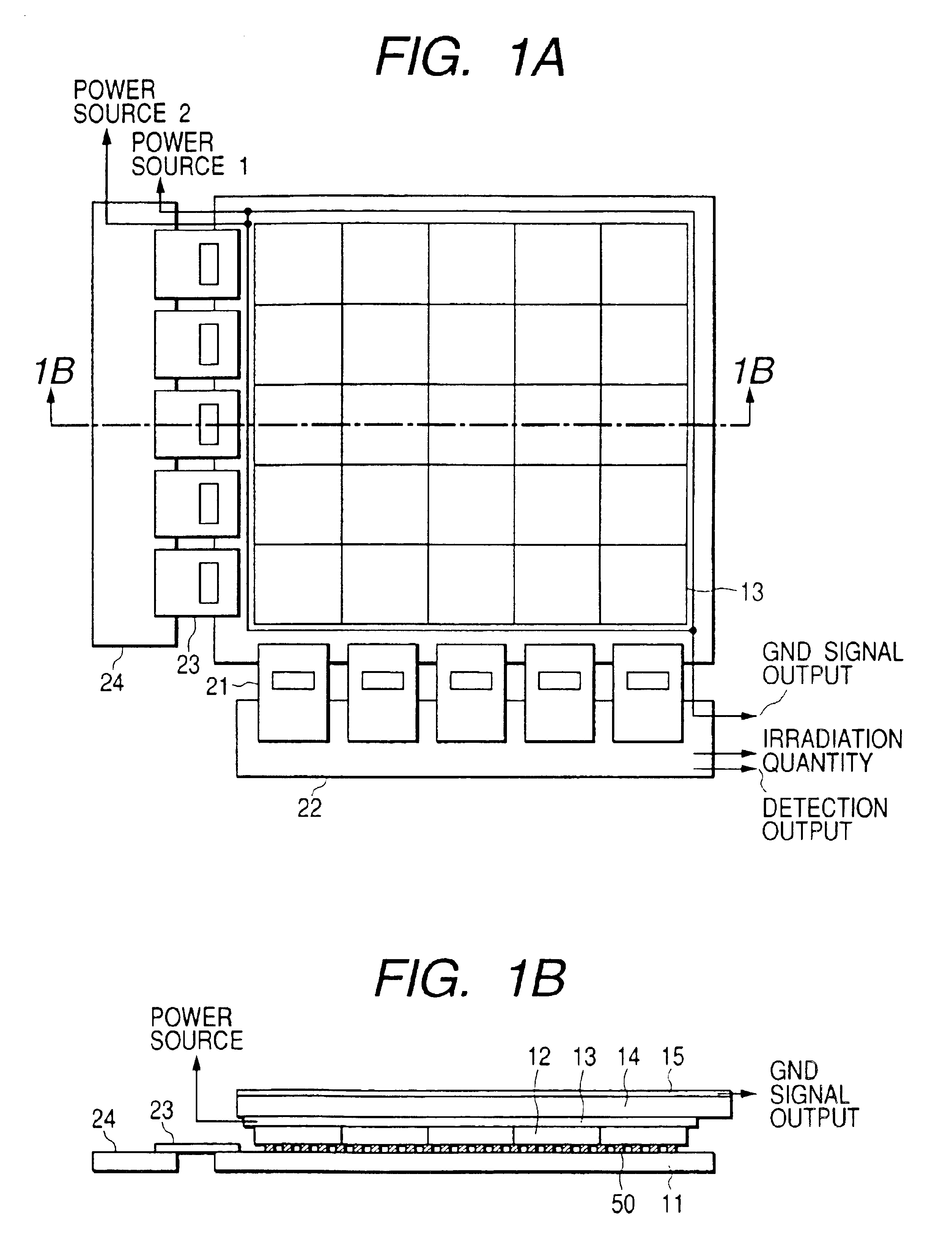
FIGS. 1A and 1B show the structure of an electromagnetic wave transforming device in accordance with a first embodiment of the present invention, in which FIG. 1A is a plan view thereof, and FIG. 1B is a cross-sectional view taken along a line 1B—1B.
Reference numeral 11 represents a substrate where thin film transistors, capacitors and so on are formed on an insulating (glass) substrate, and the thin film transistors and the capacitors are arranged in a two-dimensional matrix.
Reference 12 denotes a semiconductor substrate having a semiconductor that directly detects a high energy radiant ray, and made of GaAs, CdTe or the like as the semiconductor.
The substrate 11 and the semiconductor substrate 12 are coupled to each other vertically for each of cells with a conductor 50.
Reference numeral 13 denotes one conductor for commonly biasing a plurality of semiconductor substrates 12. The conductor 13 may be formed in a sheet shape or a mesh shape.
Reference numeral 14 den...
second embodiment
(Second Embodiment)
FIG. 9 shows an equivalent circuit diagram of the respective sensor cells 201 in the electromagnetic transforming device according to a second embodiment.
A voltage clamp transistor 305 (hereinafter simply referred to as “transistor 305”) is inserted between the X-ray sensing section 301 and the gate of the transistor 302. A constant potential is supplied to the wiring 213, thereby being capable of holding a potential of a point 306 which is connected with the transistor 305 at an opposite side of the high voltage supply side of the X-ray sensing section 301 constant. As a result, the applied electric field of the X-ray sensing section 301 can be held constant, thereby being capable of detecting a gain with respect to the X-rays without any change. It is important to hold the potential which is supplied to the wiring 213 constant.
third embodiment
(Third Embodiment)
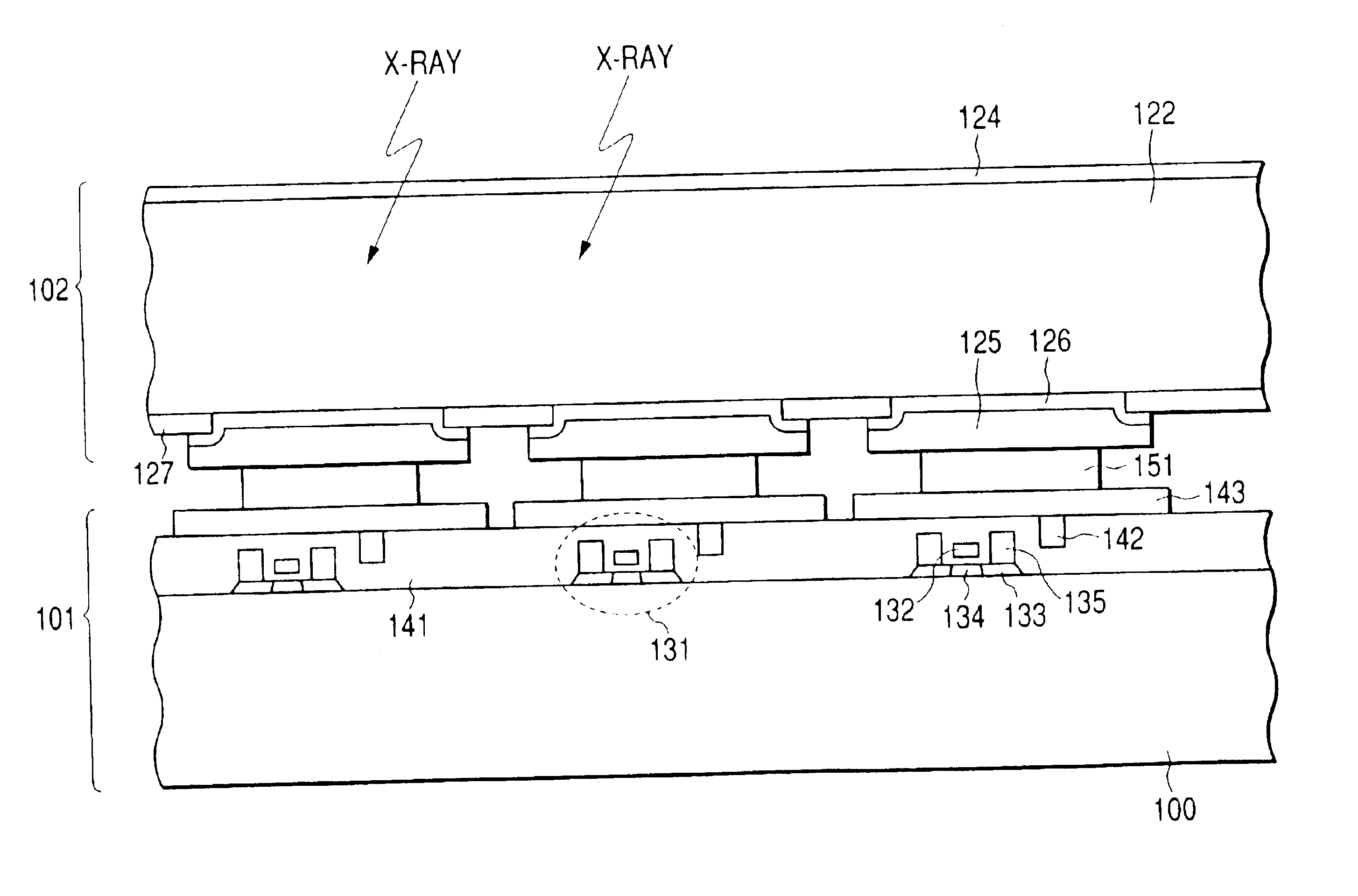
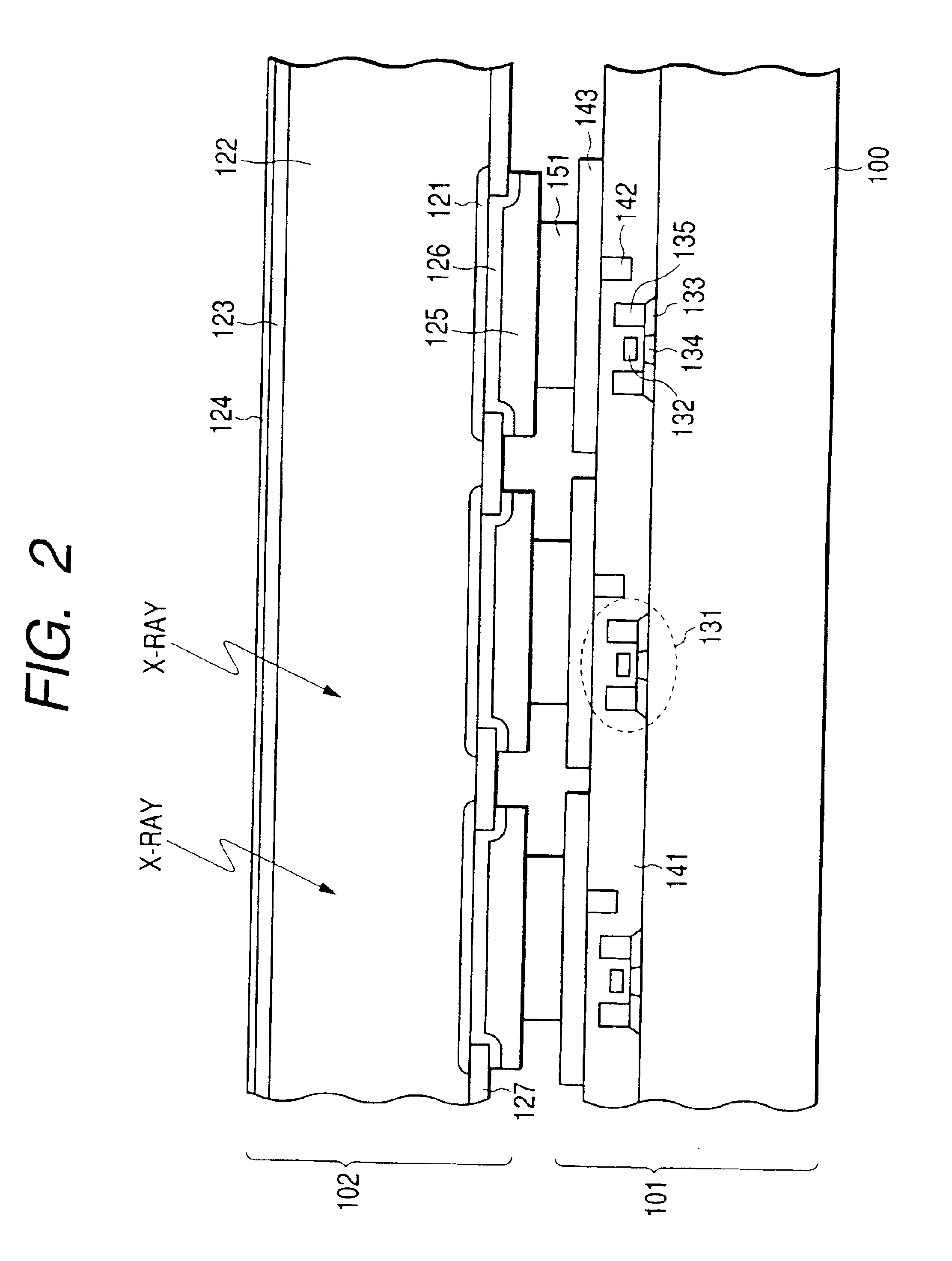
FIG. 10 is a cross-sectional view showing an electromagnetic transforming device in accordance with a third embodiment. A difference of the electromagnetic transforming device shown in FIG. 10 from the electromagnetic transforming device according to the first embodiment shown in FIGS. 1A and 1B resides in that the p+ layer 123 and the n+ layer 121 are removed, and the metal layer 124 is made of, for example, AuGeNi. The metal layer 126 is made of, for example, AuGeNi as in the first embodiment.
In this structure, the radiant rays are detected not at a pn joint portion but in the semi-insulating (i layer) semiconductor substrate.
PUM
 Abstract
Description
Claims
Application Information