Structures of and methods of fabricating trench-gated MIS devices

a technology of trench-gated mis devices and structures, which is applied in the direction of semiconductor devices, diodes, electrical apparatus, etc., can solve the problems of gate material extending outside, increasing current carrying capacity, and reducing device on-resistan

Inactive Publication Date: 2005-01-04
SILICONIX
View PDF7 Cites 101 Cited by
  • Summary
  • Abstract
  • Description
  • Claims
  • Application Information

AI Technical Summary

Benefits of technology

In accordance with another aspect of the invention, two or more protective trenches are formed on the opposite sides of the gate contact trench. This allows the gate contact tr

Problems solved by technology

All else being equal, this increases the current carrying capability and reduces the on-resistance of the device.
In the areas where the contact is to be made to the gate material, however, the gate material extends outside of the trench and overlies the surface of the silicon.
The corners of the trenches are known to be sources of stress, leading to defect-related problems in devices.
The sharper the corner, the more serious this problem becomes.
This leads to leakage currents from Fowler-Nordheim tunneling through the gate oxide and limits the maximum usable gate voltage of the devic

Method used


Image

  • Structures of and methods of fabricating trench-gated MIS devices
  • Structures of and methods of fabricating trench-gated MIS devices
  • Structures of and methods of fabricating trench-gated MIS devices

Examples


first embodiment

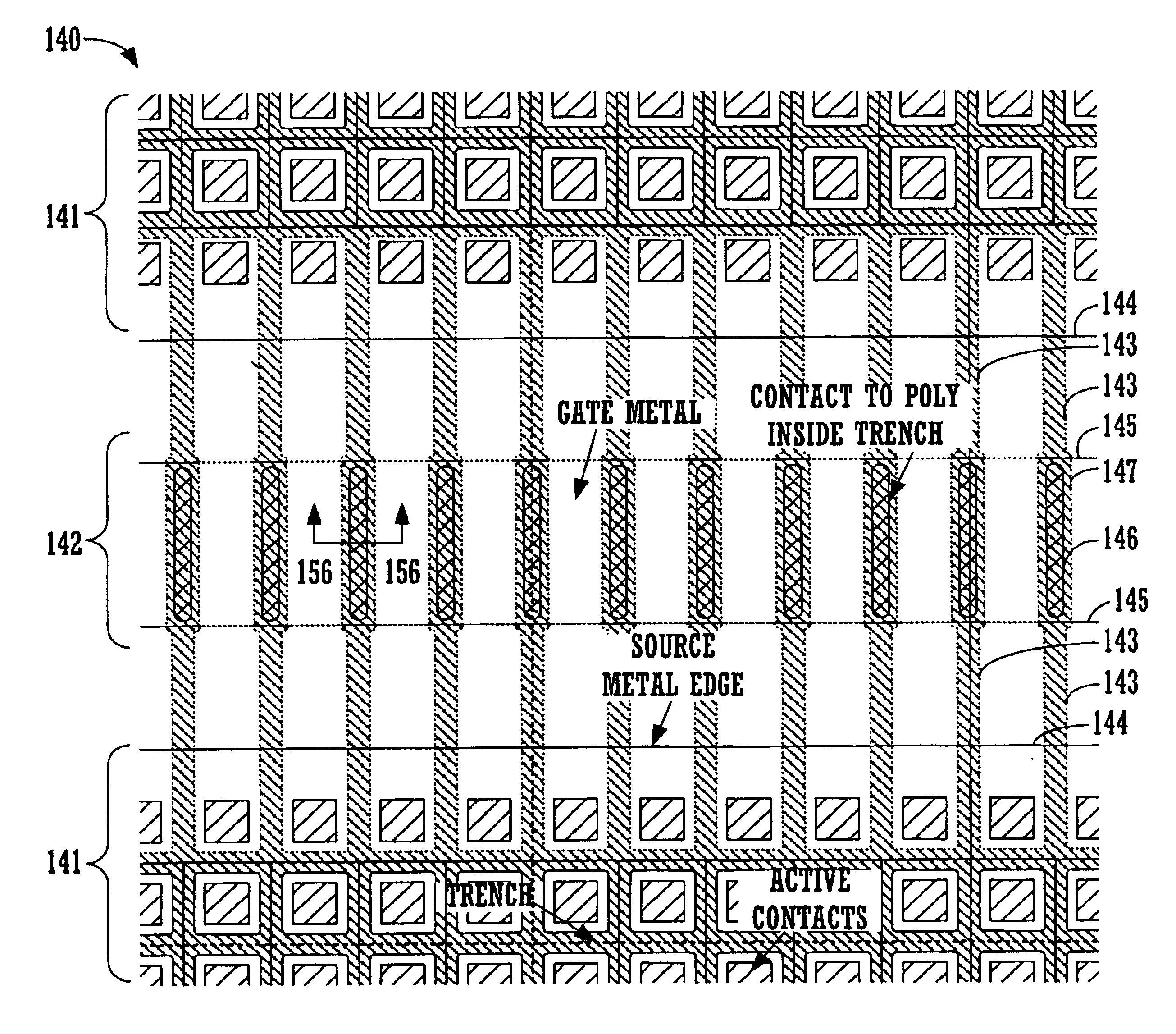
FIG. 15A shows the invention. A square-celled MOSFET 140 includes an active region 141 and a gate metal region 142. A series of parallel gate fingers 143 extend from active region 141 into gate metal region 142. The edges of the source metal are designated 144; the edges of the gate metal are designated 145. Areas 146 designate the areas of contact between the polysilicon within gate fingers 143 and gate metal 145. It will be noted that gate fingers 143 expand into wide portions 147 to accommodate areas of contact 146. This allows for a good electrical contact to be made in the trench, spaced from the upper corners of the trench, even though the dimensions of the active cells become very small. FIG. 15C shows a cross-sectional view of one of the areas of contact 146 at cross-section 15C-15C, showing a gate metal 148 and a BPSG layer 149. FIG. 15B shows a top view of a portion of MOSFET 140 that adjoins a termination region 150 and a gate pad 151.

second embodiment

FIG. 16A shows the invention. MOSFET 160 contains an active region 161 and a gate metal region 162. The edge of the source metal is shown as 164 and the edge of gate metal 168 is shown as 165. A series of parallel gate fingers 163 extend from active region 161 into gate metal region 162. An area of contact 166 between the gate polysilicon and gate metal 168 is made in a gate finger 167 which extends perpendicular to gate fingers 163. In this embodiment, gate finger 167 is wider than gate fingers 163, but this need not be the case. FIG. 16C shows a detailed cross-sectional view taken at cross-section 16C-16C in FIG. 16A. FIG. 16B is a top view of MOSFET 160 in the vicinity of a termination region 170 and a gate pad 171.

There could be problems in filling the trench at the intersections between gate fingers 163 and gate finger 167, inasmuch as gate finger 167 is wider than gate fingers 163. This possible problem is illustrated in FIGS. 16C-16F. FIG. 16C is a detailed top view of the an...

third embodiment

This problem can be overcome in the third embodiment, shown in FIGS. 17A and 17B. MOSFET 180 is similar to MOSFET 160 shown in FIGS. 16A and 16B, except that gate fingers 183 are more widely spaced than gate fingers 163, and gate finger 187 becomes narrower at the intersections with gate fingers 183. Areas of contact 186 between the gate polysilicon and the gate metal do not extend into the areas where gate fingers 183 and 187 intersect. Thus the possible problem caused by the width of gate finger 187 at the intersections with gate fingers 183 is avoided. Of course, the spacing between gate fingers 183 is variable and need not be greater than the spacing between gate fingers 163 in MOSFET 160. FIG. 17B is a top view of MOSFET 180 in the vicinity of termination region 190 and gate pad 191.


PUM


Abstract

In a trench-gated MIS device contact is made to the gate within the trench, thereby eliminating the need to have the gate material, typically polysilicon, extend outside of the trench. This avoids the problem of stress at the upper corners of the trench. Contact between the gate metal and the polysilicon is normally made in a gate metal region that is outside the active region of the device. Various configurations for making the contact between the gate metal and the polysilicon are described, including embodiments wherein the trench is widened in the area of contact. Since the polysilicon is etched back below the top surface of the silicon throughout the device, there is normally no need for a polysilicon mask, thereby saving fabrication costs.

Description

FIELD OF THE INVENTIONThis invention relates to metal-insulator-silicon semiconductor devices and in particular to such devices in which the gate is formed in a trench.BACKGROUND OF THE INVENTIONThere is a class of metal-insulator-silicon (MIS) devices in which the gate is formed in a trench that extends downward from the surface of the silicon or other semiconductor material. The current flow in such devices is primarily vertical and as a result the cells can be more densely packed. All else being equal, this increases the current carrying capability and reduces the on-resistance of the device. Devices that fit into the general catagory of MIS devices include metal-oxide-silicon field-effect transistors (MOSFETs), insulated gate bipolar transistors (IGBTs) and MOS-gated thyristors. Cross-sectional views of a single gate trench in a MOSFET, an IGBT and a MOS-gated thyristor are shown in FIGS. 1, 2 and 3, respectively.In such devices the gate material, often polysilicon, must be conn...

Claims


Application Information

Patent Timeline
IPC IPC(8): H01L29/66H01L29/78H01L21/70H01L21/336H01L21/02H01L21/768H01L21/8234H01L27/085H01L27/088H01L27/08H01L29/02H01L29/10H01L29/423H01L29/40H01L29/06H01L27/06H01L29/41H01L29/49H01L29/872
CPCH01L21/823487H01L27/088H01L29/4236H01L29/4238H01L29/66734H01L29/7811H01L29/7813H01L29/42372H01L2924/0002H01L29/0661H01L29/1095H01L29/402H01L29/407H01L29/7803H01L29/7804H01L29/7806H01L29/8725Y10S257/905H01L2924/00
Inventor BHALLA, ANUPPITZER, DORMANKOREC, JACEKSHI, XIAORONGLUI, SIK
Owner SILICONIX
Why Eureka
Try Eureka