ESD implantation in deep-submicron CMOS technology for high-voltage-tolerant applications

a technology of cmos and deep submicrons, applied in the field of semiconductor devices, can solve the problems of ldd region with a far shallower junction depth, unexpected leakage current from the output pad, and mos devices scaled down and thinner gate oxide become more vulnerable to esd stress

Inactive Publication Date: 2005-01-04
TAIWAN SEMICON MFG CO LTD
View PDF23 Cites 36 Cited by
  • Summary
  • Abstract
  • Description
  • Claims
  • Application Information

AI Technical Summary

Problems solved by technology

ESD (electrostatic discharge) damage has become one of the main reliability concerns on the IC (integrated circuit) products.
Especially, while the CMOS technology is developed into the deep-submicron regime, the scaled-down MOS devices and thinner gate oxide become more vulnerable to ESD stress.
So, the LDD region with a far shallower junction depth is easily damaged by the ESD current to cause a far lower ESD level on the output NMOS device.
If the output NMOS device in the tri-state condition must sustain high voltage input signals on the pad, the lower junction breakdown voltage due to the additional ESD implantation may cause an unexpected leakage current from the output pad to ground through the low-breakdown junction in the NMOS device.
ESD (electrostatic discharge) damage has become a main reliability concern on the IC (integrated circuit) products.
Especially, while the CMOS technology is developed into the deep-submicron regime, the scaled-down MOS devices and thinner gate oxide become more vulnerable to ESD stress.
While th

Method used


Image

  • ESD implantation in deep-submicron CMOS technology for high-voltage-tolerant applications
  • ESD implantation in deep-submicron CMOS technology for high-voltage-tolerant applications
  • ESD implantation in deep-submicron CMOS technology for high-voltage-tolerant applications

Examples


Embodiment Construction

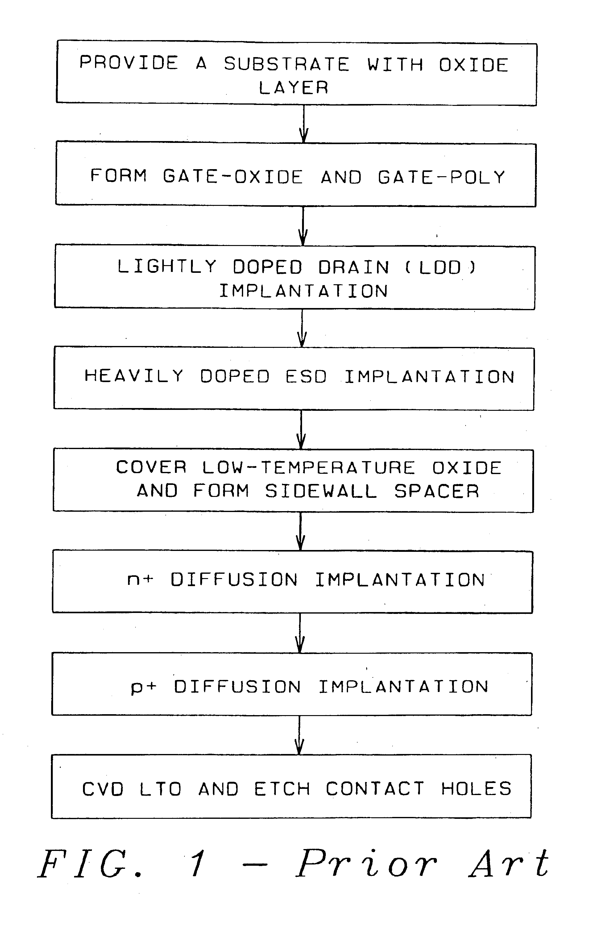
FIG. 5 is a process flow chart in accordance with this invention for high-voltage-tolerant I / O devices. FIGS. 6A-6H illustrate cross-sectional views of ESD protection NMOS devices and internal NMOS devices in accordance with this invention which show the results of the steps of FIG. 5.

FIG. 5 shows a flowchart of a process in accordance with this invention for forming a device 60 by the steps illustrated by FIGS. 6A-6H.

FIGS. 6A-6H are cross-sectional views of the FIG. 5 process flow in which the left-hand portions of FIGS. 6A-6H show the ESD protection devices and the right-hand portions of FIGS. 6A-6H show the internal devices.

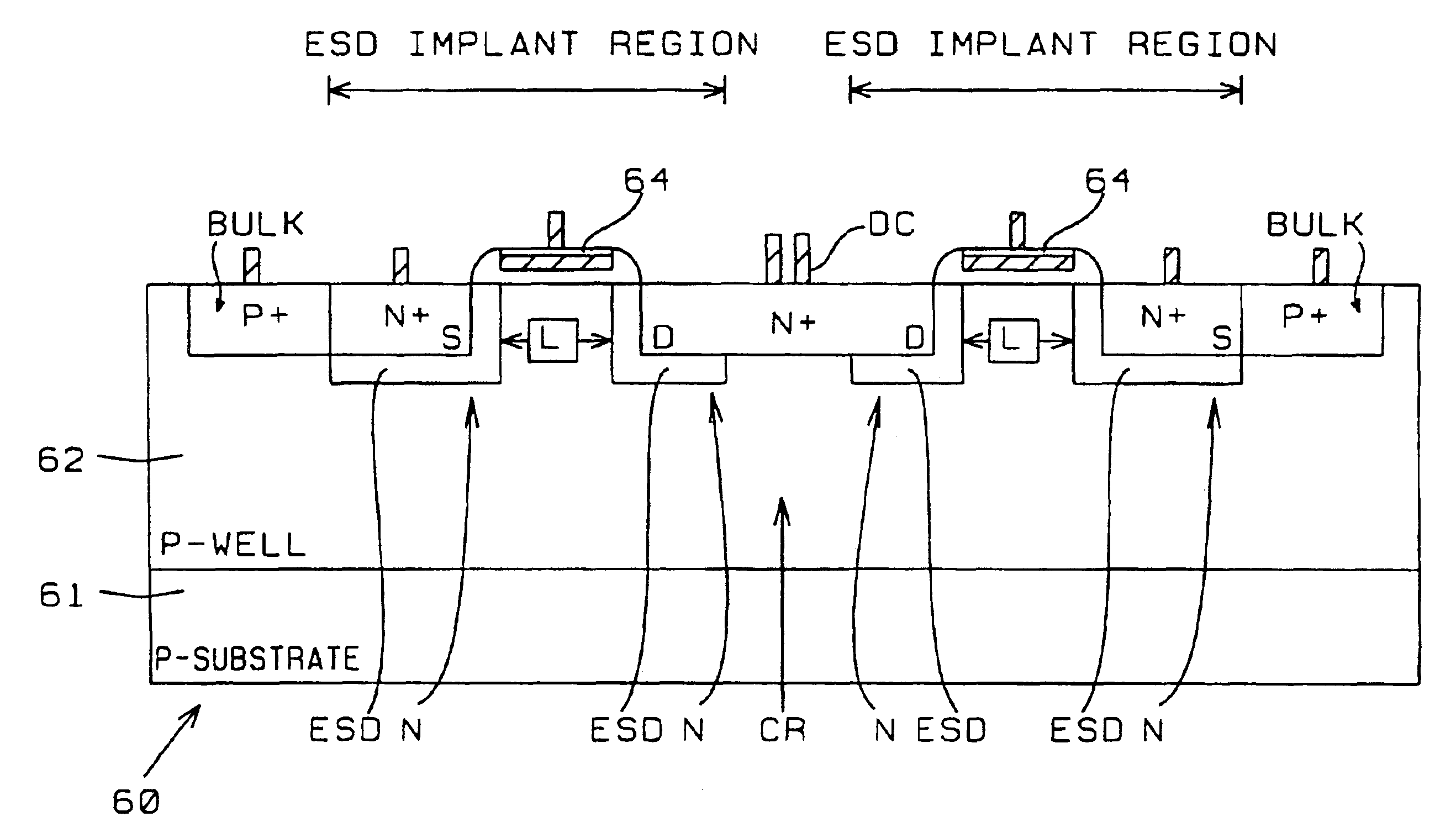
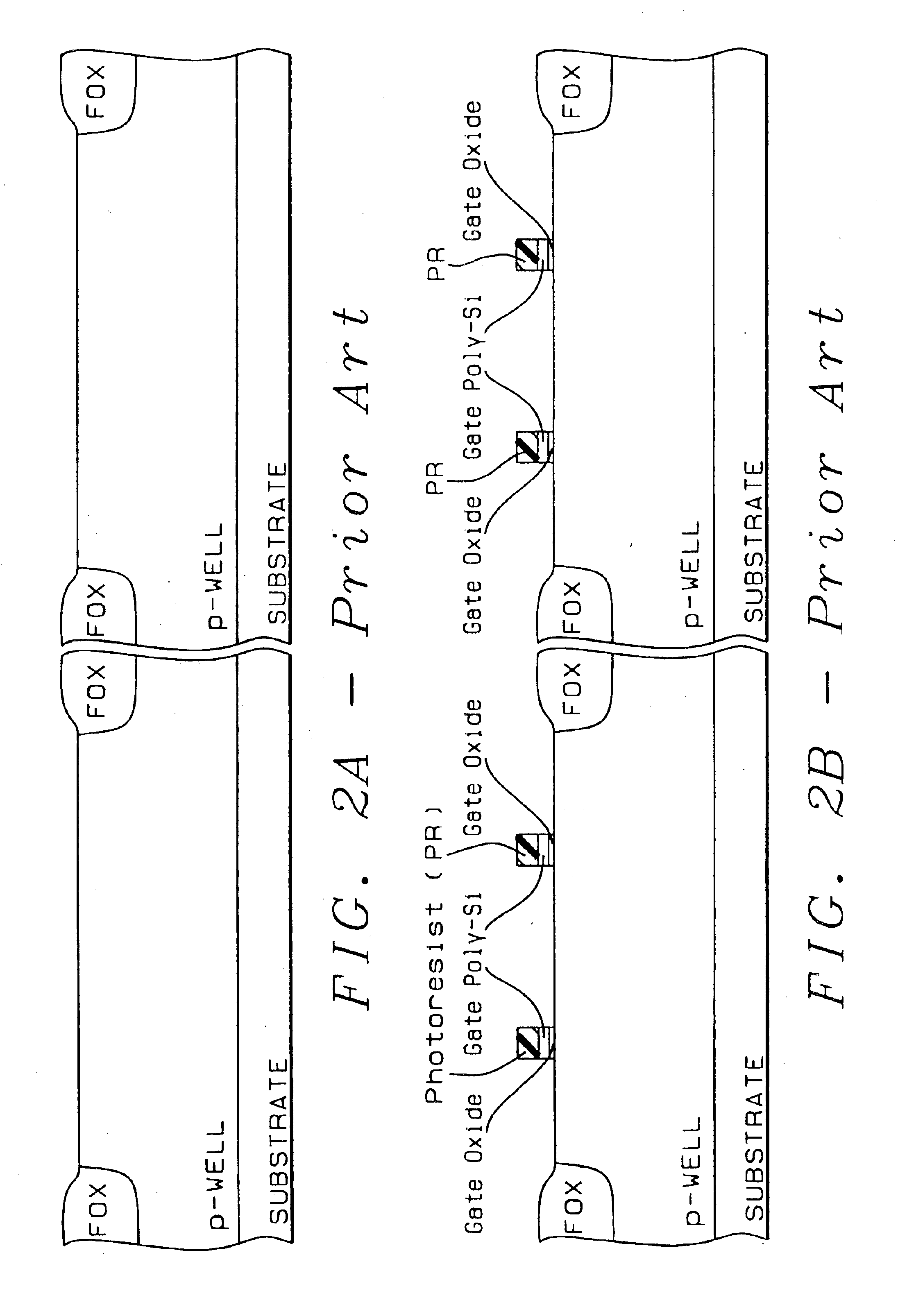
In FIG. 6A, a substrate 61 is shown with Field Oxide (FOX) regions 63 formed on the surface of a P-well 62 which frame ESD protection device region ESD and Internal Device region ID. The process of FIG. 5 starts with device 60 formed on substrate 61 including P-well 62 as shown in FIG. 6A with an ESD-Protection-Device portion ESD on the left and an internal de...


PUM


Abstract

High-voltage-tolerant ESD protection devices (ESDPD) for deep-submicron CMOS process were activated between LDD implanting and forming sidewall spacers. ESD-Implant (ESDI) regions are located at the ESDPD, without covering the center region under the drain contact (DC). The ESDI LDD concentration and doping profile are deep to contain drain diffusion. Regions with the ESDI have a high junction breakdown voltage (JBV) and a low junction capacitance. After forming gate sidewall spacers, high doping concentration ions implanted into active D/S regions formed a shallower doping profile of the D/S diffusion. The drain has a JBV as without this ESDI, so the ESD current (ESDC) is discharged through the center junction region under the DC to bulk, far from the ESDPD surface channel region. The ESDPD sustains a high ESD level. In an original drain JBV of an MOS this ESDI method is unchanged, i.e. the same as that having no such ESDI, so it can be used in I/O circuits with high-voltage signals in the deep-submicron CMOS. The ESD level of the IO ESDPD improves. The ESD discharge current path in the MOS device structure improves the ESD level in the output buffer MOS. ESDI regions are located at the output MOS devices, without covering the region under the DC. Regions under the DC without this ESDI have an unchanged JBV, so the ESDC discharges through the junction region under the DC to bulk. The original drain JBV of the output MOS with this ESDI method is unchanged, which is still the same as that having no such ESDI, to be used in the I/O circuits with high-voltage (5V) input signals in the deep-submicron CMOS with 3.3V or 2.5V VDD. This applies to diodes, FOD and lateral BJT devices.

Description

(C) STATEMENT REGARDING FEDERALLY SPONSORED RESEARCH OR DEVELOPMENT(Not Applicable)(d) INCORPORATION BY REFERENCE(Not Applicable)(e) BACKGROUND OF THE INVENTION1. Field of the InventionThis invention relates to semiconductor devices and more particularly to methuds and apparatus for protection of semiconductor devices from electrostatic discharge damage.2. Description of Related ArtESD (electrostatic discharge) damage has become one of the main reliability concerns on the IC (integrated circuit) products. Especially, while the CMOS technology is developed into the deep-submicron regime, the scaled-down MOS devices and thinner gate oxide become more vulnerable to ESD stress. For general industrial specification, the input and output pins of the IC products have to sustain the human-body-model ESD stress of above 2000V. Thus, the ESD protection circuits have to be placed around the input and output pads of the IC devices to protect the IC devices against the ESD damage.In the deep-sub...

Claims


Application Information

Patent Timeline
IPC IPC(8): H01L21/70H01L21/8238H01L21/8249H01L21/8222H01L27/02H01L29/78
CPCH01L21/8222H01L21/823814H01L21/8249H01L29/7833H01L27/0266
Inventor KER, MING-DOUCHEN, TUNG-YANGCHANG, HUN-HSIEN
Owner TAIWAN SEMICON MFG CO LTD
Why Eureka
Try Eureka