Method of selectively making copper using plating technology

a technology of plating and copper, applied in the direction of semiconductor/solid-state device manufacturing, basic electric elements, electric devices, etc., can solve the problems of not providing a means for preventing cu dishing, the first cmp step used to remove the seed layer on the surface of the substrate can be difficult to control, etc., and achieve good cmp uniformity

Inactive Publication Date: 2005-01-11
TAIWAN SEMICON MFG CO LTD
View PDF11 Cites 23 Cited by
  • Summary
  • Abstract
  • Description
  • Claims
  • Application Information

AI Technical Summary

Benefits of technology

An objective of the present invention is to provide an improved method for fabricating copper wiring that affords good CMP uniformity during planarization of a copper interconnect layer.
A further objective of the present invention is to provide an improved method of forming copper wiring that involves an electrochemical deposition and which prevents a CMP step used to polish a copper seed layer from punching through a diffusion barrier layer into a dielectric layer.
A conformal diffusion barrier layer is deposited on the electroconductive (EC) layer and on the sidewalls and bottom of the opening. Next, a copper seed layer is formed on the diffusion barrier layer and is removed above the EC layer by a first CMP step. The presence of the EC layer prevents the first CMP process from eroding the dielectric layer in situations where the thin diffusion layer is entirely removed above the dielectric layer. The EC layer functions as a stop layer since it preferably has a slower polish rate than the adjacent diffusion barrier layer and copper seed layer. A copper layer that will become an interconnect is selectively deposited by an electrochemical process on the remaining copper seed layer to fill the opening. A second CMP step is performed to lower the level of the copper layer until it is coplanar with the dielectric layer. In so doing, the EC layer and the diffusion barrier layer above the dielectric layer are removed and a copper interconnect is completed with good uniformity and improved performance.

Problems solved by technology

It should be noted that as the width of via holes or trench openings is shrinking in new technologies, the difficulty in forming a uniform thin diffusion barrier layer has resulted in adopting new techniques that include atomic layer deposition (ALD).
However, a first CMP step that is used to remove the seed layer on the surface of the substrate can be difficult to control since the underlying diffusion barrier layer is frequently too thin to function as a good CMP stop.
However, the method does not provide a means for preventing Cu dishing.

Method used


Image

  • Method of selectively making copper using plating technology
  • Method of selectively making copper using plating technology
  • Method of selectively making copper using plating technology

Examples


first embodiment

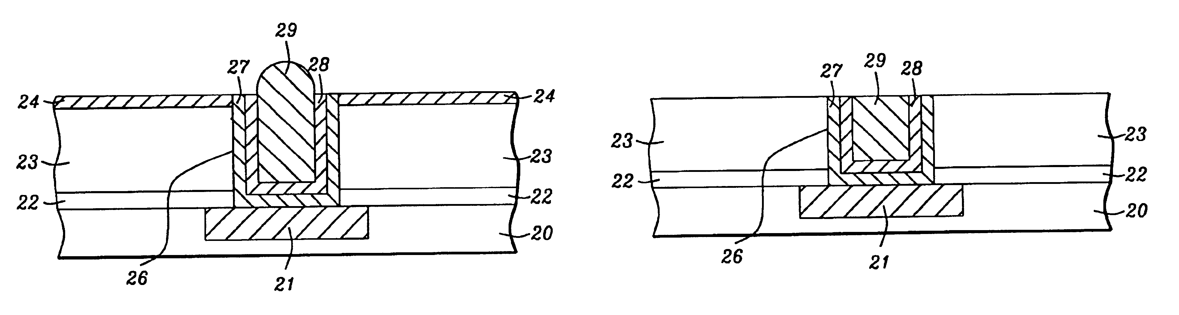
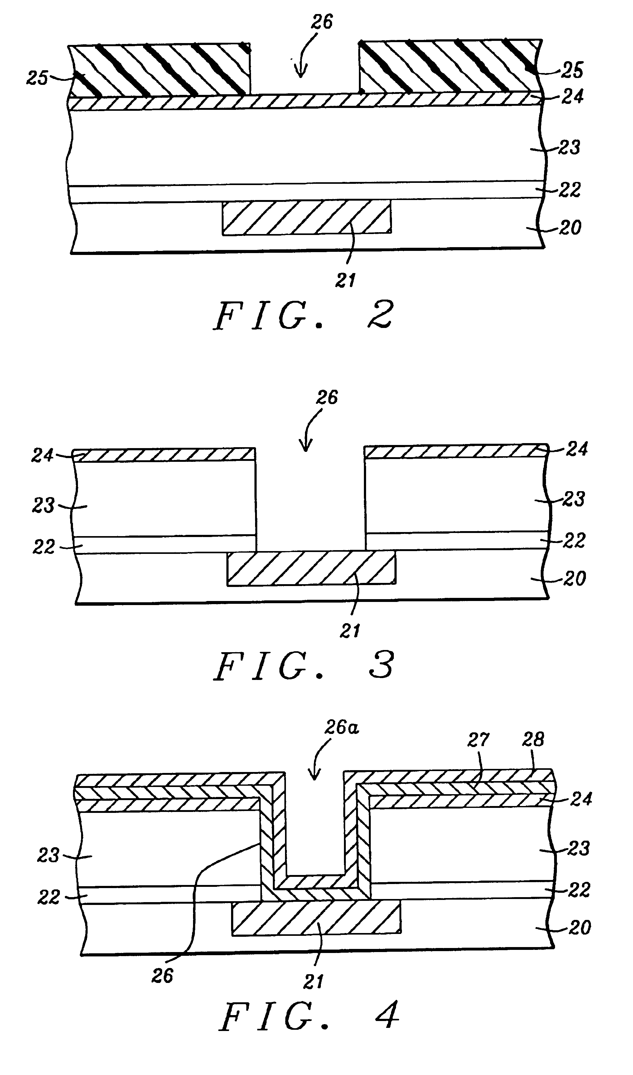
The present invention is particularly useful in forming metal wiring with improved uniformity and high performance in an integrated circuit that is part of a microelectronic device. Preferably, the metal is copper and the copper wiring may be in the form of an interconnect that is fabricated by a single or dual damascene scheme. However, another metal or a metal alloy may be used to form an interconnect. A first embodiment is depicted in FIGS. 2-7. Although the figures depict a single damascene sequence, it should be understood that the invention is equally effective in a dual damascene method that involves a via first approach where a trench is formed above a via. Furthermore, the figures are not necessarily drawn to scale and are not intended to limit the scope of the invention.

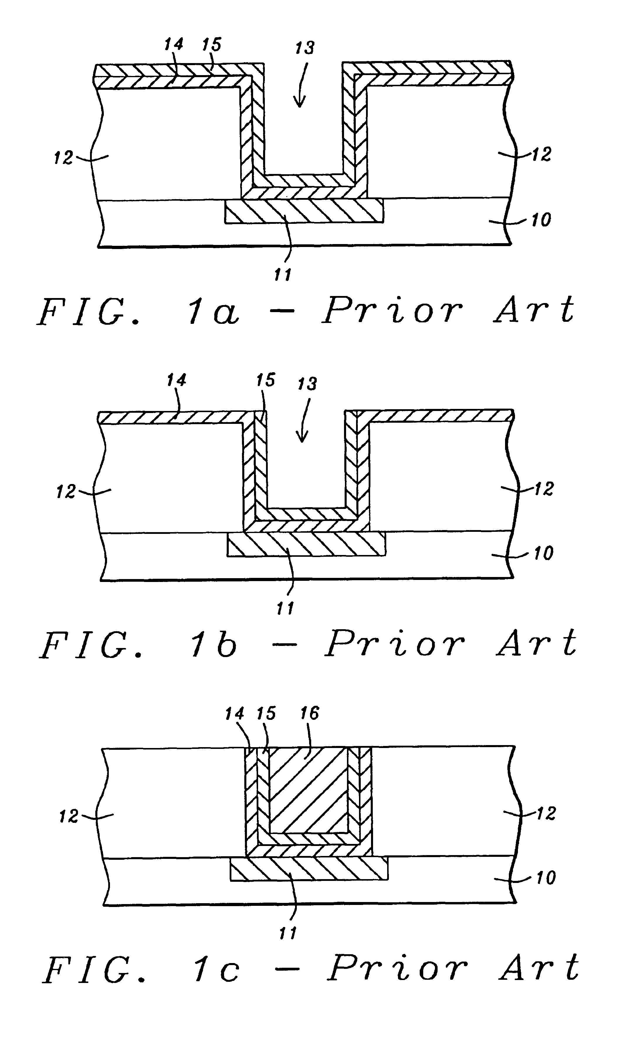
As a background to the present invention, the inventors have previously practiced a copper wiring method as represented in FIGS. 1a-1c. Referring to FIG. 1a, a substrate 10 is provided that is typically sil...


PUM

PropertyMeasurementUnit
thicknessaaaaaaaaaa
widthaaaaaaaaaa
thicknessaaaaaaaaaa

Abstract

A method of forming a more uniform copper interconnect layer is described. A dielectric layer, electroconductive (EC) layer, and a photoresist layer are sequentially deposited on a substrate. An opening in the photoresist is etched through the dielectric layer while the EC layer serves as a hard mask. Following deposition of a diffusion barrier layer and copper seed layer on the EC layer and in the opening, the copper seed layer is removed above the EC layer by a first CMP step. The EC layer serves as a CMP stop to protect the dielectric layer and provides a more uniform surface for subsequent steps. Copper is selectively deposited on the seed layer within the opening. A second CMP step lowers the copper layer to be coplanar with the dielectric layer and removes the EC layer. The resulting copper interconnect layer has a more uniform thickness and surface for improved performance.

Description

FIELD OF THE INVENTIONThe invention relates to a method of fabricating a copper interconnect with improved performance and in particular to a method of forming an electroconductive layer that serves as a hard mask during an etch transfer step and as a stop layer during a chemical mechanical polish step.BACKGROUND OF THE INVENTIONThe manufacture of integrated circuits in a semiconductor device involves the formation of a sequence of layers that contain metal wiring. Metal wiring that forms interlevel and intralevel connections in a device is insulated by one or more dielectric layers in order to prevent crosstalk between the electrical pathways which can degrade device performance. A popular method of forming metal wiring is a damascene process in which a metal is deposited in an opening such as a via hole or a trench above a via in a dielectric layer. Usually, a conformal diffusion barrier layer is formed between the metal layer and dielectric layer to protect the metal from corrosi...

Claims


Application Information

Patent Timeline
Patent Type & Authority Patents(United States)
IPC IPC(8): H01L21/70H01L21/768
CPCH01L21/76879H01L21/7684
Inventor YU, CHEN-HUATSENG, HORNG-HUEI
Owner TAIWAN SEMICON MFG CO LTD
Why Eureka
Try Eureka