Semiconductor package board using a metal base

a technology of semiconductor package board and metal base, which is applied in the direction of printed circuit manufacturing, printed circuit electric connection formation, printed circuit aspects, etc., can solve the problems of defective products, affecting the yield of ceramic multi-layer wiring board, and prone to chipping or cracking during fabrication and transfer, and achieves high reliability and superior smoothness.

Inactive Publication Date: 2005-01-11
NEC CORP
View PDF15 Cites 31 Cited by
  • Summary
  • Abstract
  • Description
  • Claims
  • Application Information

AI Technical Summary

Benefits of technology

[0014]In view of the above-described problems in the prior art, it is an object of the present invention to provide an improved semiconductor package board with superior smoothness, and a manufacturing method thereof, for providing a highly reliable semiconductor device which enables further miniaturization of high-pin-contact, high-density circuit, and which requires no stiffener.
[0016]According to the semiconductor package board of the present invention, the multilayer wiring film is laminated on the flat metal base, whereby smoothness of the multilayer wiring film is improved. The metal base also serves to reinforce the multilayer wiring film, so as to restrict deformation thereof and to allow circuits to have a higher density and a smaller width with more pins.
[0018]According to the semiconductor device of the present invention, the semiconductor chip is received in the opening formed in the metal base and connected on the top surface of the multilayer wiring film, whereby the reliability of the connection between the semiconductor chip and the multilayer wiring film is improved.
[0020]According to the method of the present invention, the multilayer wiring film is laminated on a planar metal base which serves as a support, after which the opening is formed in the metal base in a region in which the semiconductor chip is to be received. This improves smoothness of the multilayer wiring film, particularly the smoothness of the surface thereof on which the semiconductor chip is mounted.

Problems solved by technology

However, the above-mentioned prior art has the following problems.
Ceramic used for the insulating board in the ceramic multilayer wiring board is hard and brittle, and consequently it is apt to chip or crack during fabrication and transfer.
Chipping or cracking of the board deteriorates the sealing property of the semiconductor chip rendering it defective, and leads to a decrease in the yield of the ceramic multilayer wiring boards.
There is inevitably warpage in the baked board because of the shrinkage caused by baking at a high temperature, resulting in defective products due to deformation or dimensional variations.
Such products which do not satisfy the physical requirements cannot provide a high degree of smoothness required for a high-density circuit board or a flip-chip mounting board.
That is, physical defects of the board constitute an impediment to a further increase in the number of pins or the density of the circuit and to further miniaturization of the circuit.
Poor smoothness in a region where a semiconductor chip is mounted causes cracks or disconnections between the flip-chip mounted semiconductor chip and the board.
As a result the reliability of the semiconductor device is lowered.
Build-up boards are apt to warpage because of the mismatches in the coefficient of thermal expansion between the printed circuit board used as a core material and the insulating resin film formed on the board.
Such warpage also causes various problems when flip-chip bonding a multi-pinned semiconductor chip impeding further increase in the circuit density.
Warpage also decreases the yield of the build-up board.
Tape-type boards made of polyimide have a drawback that position misalignment often occurs because of the expansion of the tape carrier, and therefore it is not suitable for higher density circuit formation.
Therefore, the region on which the semiconductor chip is mounted is often undulated because of the multi-layered structure, and consequently the connection between the semiconductor chip and the multilayer wiring structure film is unstable.
While the board can have a higher rigidity because of the stiffeners, the provision of such stiffeners makes the fabrication process more complex, and increases the production cost of the semiconductor device.

Method used


Image

  • Semiconductor package board using a metal base
  • Semiconductor package board using a metal base
  • Semiconductor package board using a metal base

Examples


first embodiment

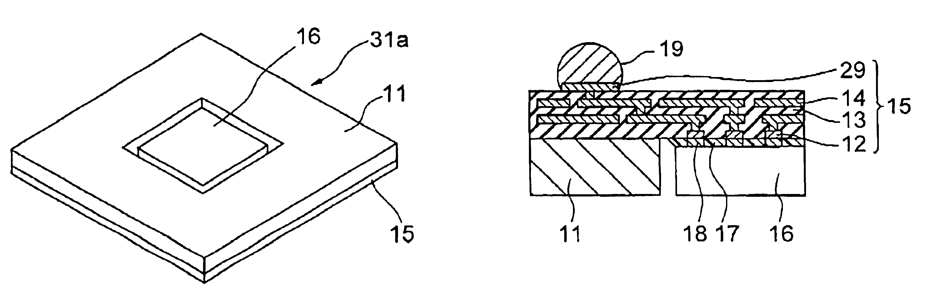
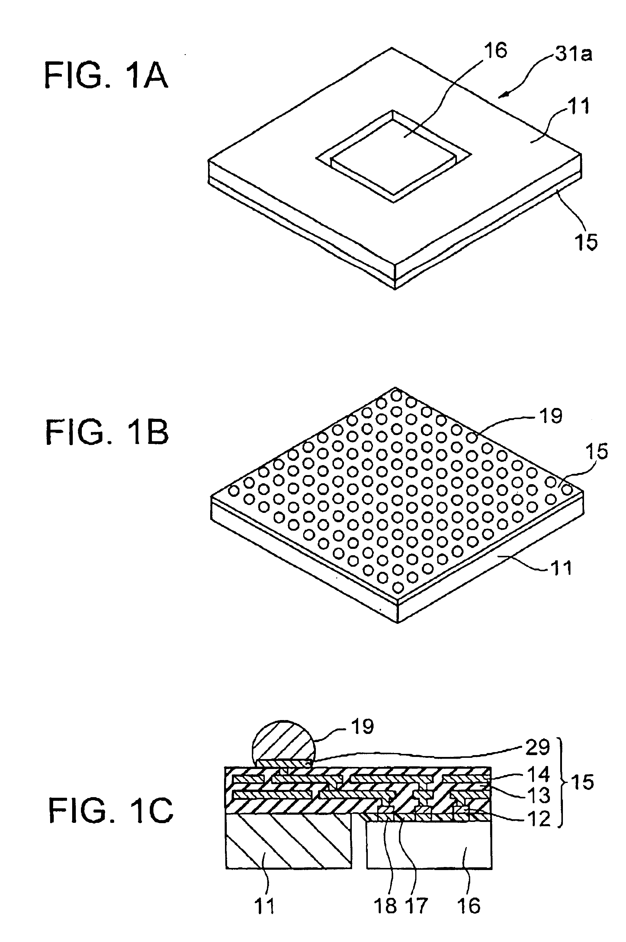
[0045]Referring to FIGS. 1A to 1C, a semiconductor device according to the present invention includes a full-grid ball grid array (BGA) chip 16 mounted on a multilayer wiring film 15 within a central opening of a metal base 11.

[0046]The metal base 11 having the central opening and the multilayer wiring film 15 mounted on the metal base 11 in combination constitute a semiconductor package board 31a of the present embodiment. The metal base 11 is formed as a metal plate attached with the multilayer wiring film 15. The opening of the metal base 11 receives therein the semiconductor chip 16, which is mounted on the multilayer wiring film 15. On the rear surface (top surface) of the multilayer wiring film 15 opposite from the front surface thereof where the metal base 11 and the semiconductor chip 16 are arranged, there are provided an array of second metal pads 29, on which an array of solder balls 19 which form a BGA structure are mounted.

[0047]On the front surface of the multilayer wi...

second embodiment

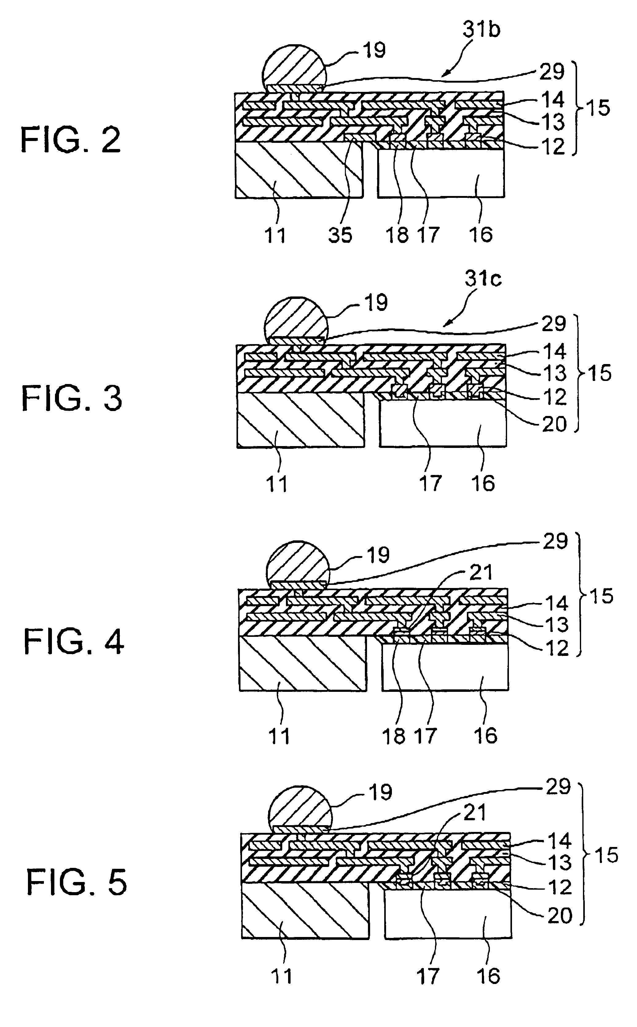
[0058]Next, a semiconductor package board or a semiconductor device according to the present invention will be described. FIG. 2 is a partial sectional view showing the structure of the semiconductor device using the semiconductor package board according to the present embodiment. The characteristic feature of the semiconductor package board according to the present embodiment is that a metallic film 35 is formed on the multilayer wiring film 15 at the periphery of the central opening of the metal base 11.

[0059]In the semiconductor device of the present embodiment, the semiconductor chip 16 is mounted on the semiconductor package board 31b within the central opening of the metal base 11. This structure is formed as follows. Specifically, the semiconductor chip 16 is disposed within the central opening of the metal base 11, and subjected to flip-chip bonding to the metal pads 12 disposed within the central opening by using solder balls 18. Subsequently, the underfill (or underfilling...

third embodiment

[0061]Next, a semiconductor package board according to the present invention will be described. FIG. 3 is a partial sectional view showing the structure of the semiconductor device using the semiconductor package board according to the present embodiment. The characteristic feature of the semiconductor package board according to the present embodiment is that solder balls 20 are provided on the surface of the metal pads 12 so as to protrude from the surface of the multilayer interconnection film 15.

[0062]The semiconductor device according to the third embodiment of the present invention includes a semiconductor package board 31c and a semiconductor chip 16 mounted thereon, and is assembled as follows. The semiconductor chip 16 is flip-chip bonded through solder balls 20 to the metal pads 12 arranged within the opening in the metal base 11 The semiconductor chip 16 may have the solder balls 18, in which case it is connected to the metal pads 12 through both the solder balls 18 and 20...


PUM


Abstract

A semiconductor package board for mounting thereon a semiconductor chip includes a metal base having an opening for receiving therein the semiconductor chip and a multilayer wiring film layered onto the metal base. The semiconductor chip is flip-chip bonded onto the metal pads disposed on the multilayer wiring film within the opening. The surface of the metal base is flush with the top surface of the semiconductor chip received in the opening. The resultant semiconductor device has a larger number of external pins and a smaller deformation without using a stiffener.

Description

BACKGROUND OF THE INVENTION[0002](a) Field of the Invention[0003]The present invention relates to a semiconductor package board using a metal base, a semiconductor device using the semiconductor package, and a manufacturing method thereof More specifically, the present invention relates to a semiconductor package board having excellent smoothness in a part on which a semiconductor chip is mounted, thereby improving reliability of the semiconductor device, and to a manufacturing method of such semiconductor package board.[0004](b) Description of the Related Art[0005]Ceramic multilayer wiring boards, each of which mounts thereon a semiconductor chip, for example, enable high-density interconnections to be formed and are widely used. Such ceramic multilayer wiring boards are described in Japanese Patent Laid-open Publication No. Hei. 8-330474. The ceramic multilayer wiring board described in this publication includes an insulating board made of alumina or the like on which a conductor ...

Claims


Application Information

Patent Timeline
Patent Type & Authority Patents(United States)
IPC IPC(8): H01L21/02H01L21/60H01L23/538H01L23/48H01L23/498H01L23/52H05K3/44H05K3/06H05K3/00H05K3/40H05K3/20H05K3/46
CPCH01L21/4857H01L23/49811H01L23/49816H01L23/49827H01L23/49833H01L23/5389H01L24/81H05K3/44H05K3/4682H01L24/19H01L2924/01327H01L2224/73204H01L2224/81801H01L2924/01013H01L2924/01029H01L2924/01057H01L2924/01073H01L2924/01079H01L2924/19041H01L2924/19043H05K3/0097H05K3/06H05K3/20H05K3/205H05K3/4007H05K3/4644H05K2201/0367H05K2201/0969H05K2203/0323H05K2203/0376H05K2203/061H05K2203/1536H01L2924/01005H01L2924/01033H01L2924/01042H01L2924/01047H01L2924/0105H01L2924/01074H01L2924/01078H01L2924/014H01L21/6835H01L2924/12042H01L2924/00
Inventor KIKUCHI, KATSUMISHIMOTO, TADANORIMATSUI, KOJIBABA, KAZUHIRO
Owner NEC CORP
Why Eureka
Try Eureka