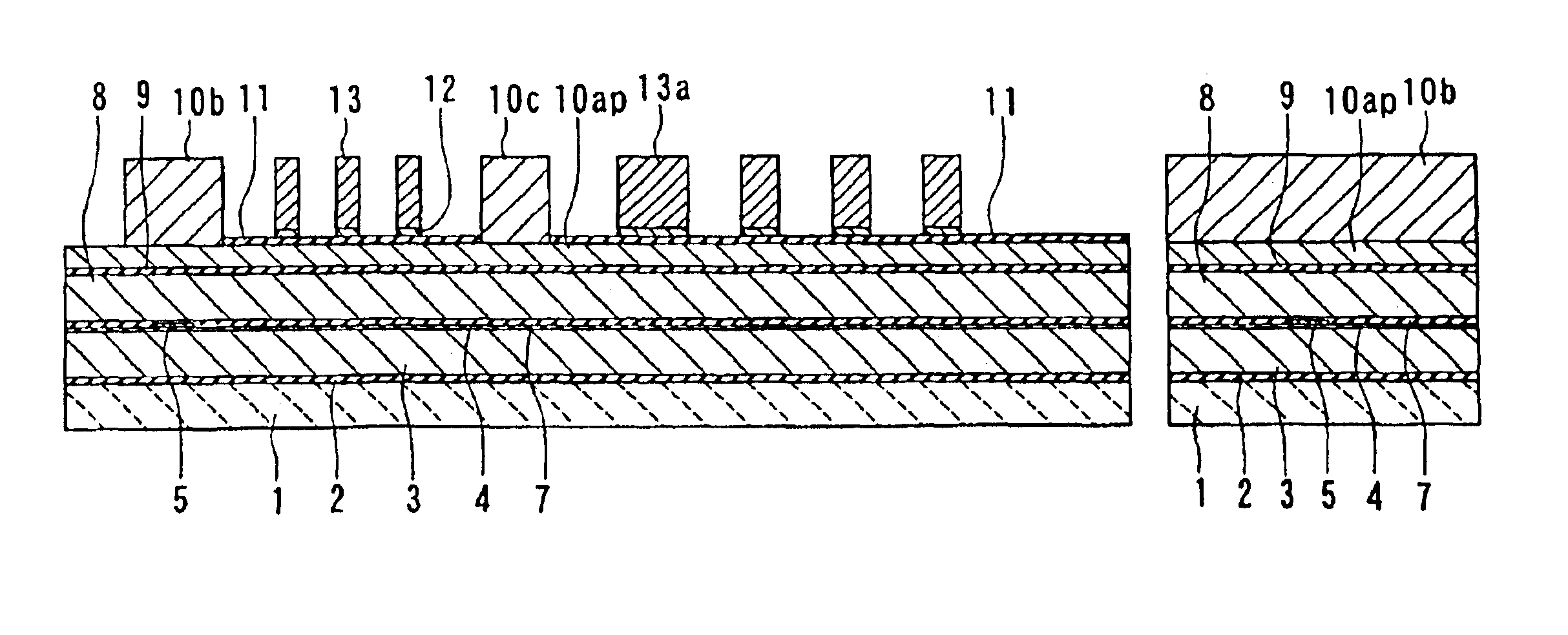
Thin-film magnetic head including thin-film coil and lead layer connected via connecting layer
a thin-film coil and magnetic head technology, applied in the field of manufacturing a thin-film magnetic head, can solve the problems of difficult to form a fine frame with precision, difficult to generate a high-density magnetic flux between, etc., to achieve excellent recording characteristics, small yoke length, and high precision
- Summary
- Abstract
- Description
- Claims
- Application Information
AI Technical Summary
Benefits of technology
Problems solved by technology
Method used
Image
Examples
first embodiment
[First Embodiment]
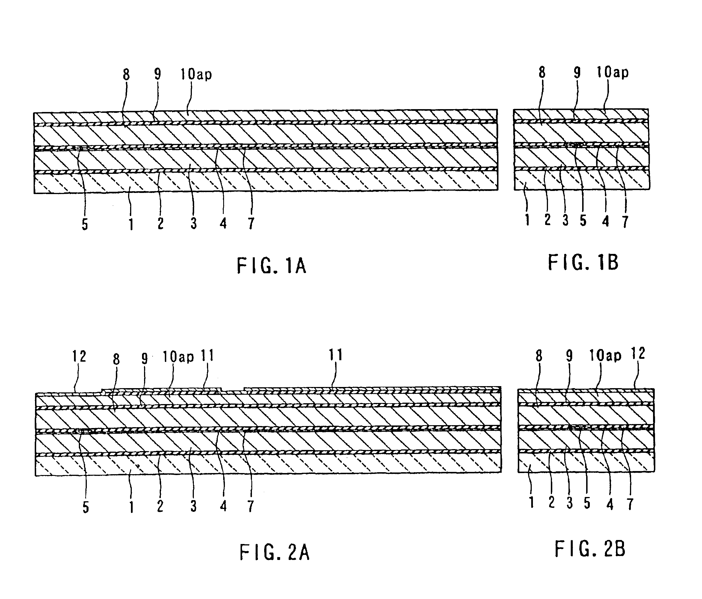
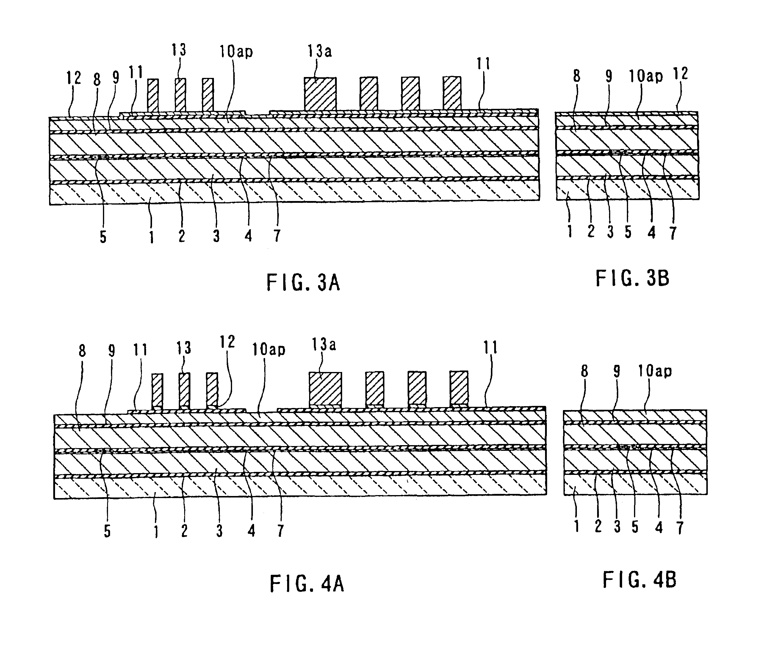
Reference is now made to FIGS. 1A to 17A and FIGS. 1B to 17B to describe a method of manufacturing a thin-film magnetic head according to a first embodiment of the invention. FIGS. 1A to 17A are cross sections each orthogonal to the air bearing surface and the top surface of the substrate. FIGS. 1B to 17B are cross sections of magnetic pole portions each parallel to the air bearing surface.
In the method of manufacturing the thin-film magnetic head of the embodiment, as shown in FIGS. 1A and 1B, an insulating layer 2 made of alumina (Al2O3), for example, is first deposited to a thickness of approximately 1 to 3 μm on a substrate 1 made of aluminum oxide and titanium carbide (Al2O3-TiC), for example. On the insulating layer 2, a bottom shield layer 3 of a magnetic material such as Permalloy is formed to a thickness of approximately 2 to 3 μm for making a reproducing head. The bottom shield layer 3 is selectively formed on the insulating layer 2 by plating using a pho...
second embodiment
[Second Embodiment]
Reference is now made to FIGS. 27A to 36A and FIGS. 27B to 36B to describe a method of manufacturing a thin-film magnetic head according to a second embodiment of the invention. FIGS. 27A to 36A are cross sections each orthogonal to the air bearing surface and the top surface of the substrate. FIGS. 27B to 36B are cross sections of the magnetic pole portions each parallel to the air bearing surface.
Up to the step of forming the inter-coil insulating film 15, the manufacturing method of this embodiment has the same steps as the foregoing ones described with reference to FIGS. 1A to 7A and FIGS. 1B to 7B.
Then, in this embodiment, as shown in FIGS. 27A and 27B, an electrode film 31 for a second thin-film coil is formed of Cu by CVD, for example, to a thickness of about 50 to 100 nm so as to cover the entire top surface of the laminate. The material of the electrode film 31 is not limited to Cu but may be Ta, W, TiN, TiW or Ti, for example.
Then, although not shown, a ...
third embodiment
[Third Embodiment]
Reference is now made to FIGS. 37A to 50A and FIGS. 37B to 50B to describe a method of manufacturing a thin-film magnetic head according to a third embodiment of the invention. FIGS. 37A to 50A are cross sections each orthogonal to the air bearing surface and the top surface of the substrate. FIGS. 37B to 50B are cross sections of the magnetic pole portions each parallel to the air bearing surface.
The manufacturing method of this embodiment is the same as that of the first embodiment up to the step of forming the magnetic layer 10ap as shown in FIGS. 1A and 1B. Then, in this embodiment, as shown in FIGS. 37A and 37B, an insulating film 41 made of alumina, for example, is formed on the magnetic layer 10ap to a thickness of 0.2 μm. Although not shown, a photoresist film is then formed on the insulating film 41 in a region in which a thin-film coil 43 described later is to be formed. Using this photoresist film as a mask, the insulating film 41 is selectively etched s...
PUM
| Property | Measurement | Unit |
|---|---|---|
| height | aaaaa | aaaaa |
| height | aaaaa | aaaaa |
| width | aaaaa | aaaaa |
Abstract
Description
Claims
Application Information


