Method for operating N-channel electrically erasable programmable logic device

a programmable logic and n-channel technology, applied in semiconductor devices, digital storage, instruments, etc., can solve the problems of large-area coupling gate, i.e., n-well /b>14/b>, and consume a lot of valuable chip area

Inactive Publication Date: 2005-01-11
EMEMORY TECH INC
View PDF4 Cites 17 Cited by
  • Summary
  • Abstract
  • Description
  • Claims
  • Application Information

AI Technical Summary

Benefits of technology

Accordingly, the primary objective of the present invention is to provide a single-poly electrically erasable prog

Problems solved by technology

However, one disadvantage of the above-described prior art single-poly EPROM 10 is tha

Method used


Image

  • Method for operating N-channel electrically erasable programmable logic device
  • Method for operating N-channel electrically erasable programmable logic device
  • Method for operating N-channel electrically erasable programmable logic device

Examples


Embodiment Construction

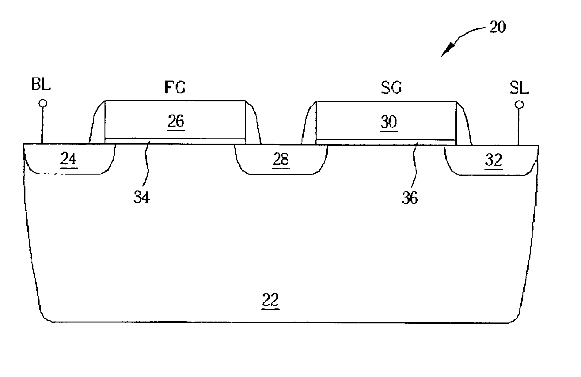
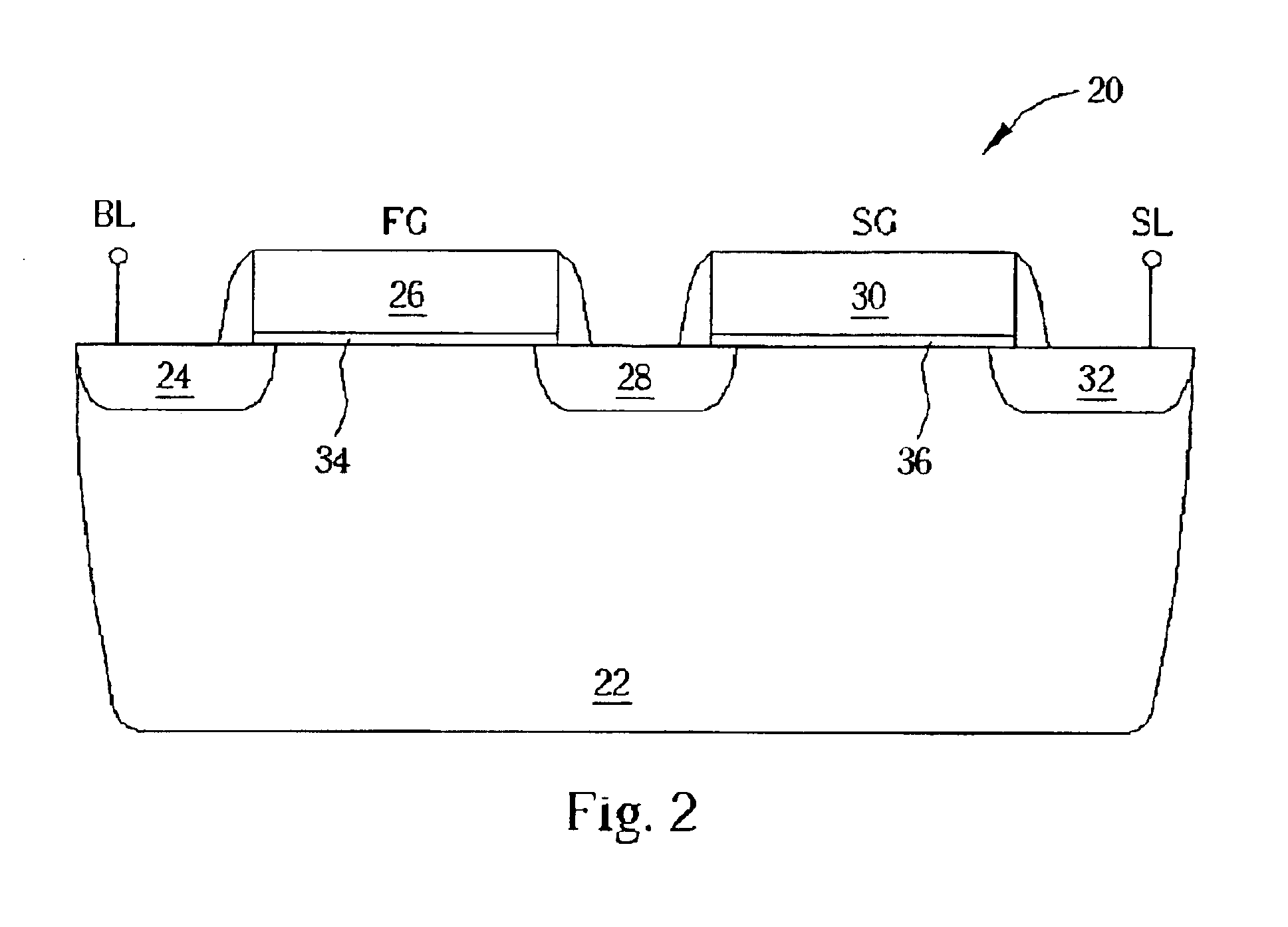
Please refer to FIG. 2. FIG. 2 is an enlarged cross-sectional view schematically showing a single-poly electrically erasable programmable logic device(EEPLD) 20 according to the present invention. As shown in FIG. 2, the EEPLD 20 comprises a P substrate 22, a first N-type ion doped area 24 electrically connected to a bit line BL, a floating gate 26 situated over the P substrate 22 next to the first N-type ion doped area 24 for storing digital data, a second N-type ion doped area 28 situated in the P substrate 22, a select gate 30 electrically connected to a word line (not shown), and a third N-type ion dope area 32 situated in the P substrate 22. A first oxide layer 34 and a second oxide layer 36 are disposed respectively between the floating gate 26 and the substrate 22 and between the select gate 30 and the substrate 22.

One preferred embodiment of the EEPLD 20 for use as a memory unit of a non-volatile memory array will be described below with reference to FIG. 3 to FIG. 8.

Please ...


PUM


Abstract

An electrically erasable programmable logic device (EEPLD) contains a P-type substrate. A first N-type doped region is disposed in the P-type substrate. A first gate, which is used to store data, overlies the P-type substrate and is adjacent to the first N-type doped region. A second N-type doped region is laterally disposed in the P-type substrate. The second N-type doped region is also adjacent to the first gate. A second gate, which acts as a select gate or select gate of the EEPLD, overlies the P-type substrate and is adjacent to the second N-type doped region. A third N-type doped region is disposed in the P-type substrate. The third N-type doped region is adjacent to the second gate. By Applying a sufficient voltage on the first N-type doped region (VBL), and changing a select gate voltage (VSG) or the third N-type doped region voltage (VSL) applied on the second gate of the EEPLD, the operation of the EEPLD can be selectively implemented either under a channel hot hole (CHH) program mode or a channel hot electron (CHE) erase mode.

Description

BACKGROUND OF INVENTION1. Field of the InventionThe present invention relates to an electrically erasable programmable logic device (EEPLD) for use as non-volatile memory. More particularly, the present invention relates to an electrically erasable programmable read only memory device capable of implementing multi-level program operations. According to the present invention, the electrically erasable programmable read only memory is compatible with standard CMOS manufacturing processes and the dimension of the electrically erasable programmable read only memory unit is shrunk.2. Description of the Prior ArtWith demands for portable electrical products in recent years, techniques of electrically erasable programmable read-only memory (EEPROM) have been matured and the market has expanded. EEPROM could be applied in digital cameras, video game consoles, personal digital assistants, recording devices of telephones, and programmable IC products. EEPROM is a non-volatile memory, which ch...

Claims


Application Information

Patent Timeline
IPC IPC(8): H01L27/115H01L29/66H01L21/70H01L21/8247H01L29/788G11C16/04
CPCG11C16/0433H01L29/7885H01L27/11521H01L27/11558H01L27/115G11C2216/10H10B41/60H10B69/00H10B41/30
Inventor LEE, KUNG-HONGHSU, CHING-HSIANGKING, YA-CHINSHEN, SHIH-JYEHO, MING-CHOU
Owner EMEMORY TECH INC
Why Eureka
Try Eureka