Multi-beam multi-column electron beam inspection system

a multi-column electron beam and electron beam technology, applied in the direction of material analysis using wave/particle radiation, instruments, nuclear engineering, etc., can solve the problems of circuit failure, limited resolution, and becoming increasingly difficult to detect defects that are smaller than the wavelength of the measuring ligh

Inactive Publication Date: 2005-01-18
MULTIBEAM CORP
View PDF26 Cites 139 Cited by
  • Summary
  • Abstract
  • Description
  • Claims
  • Application Information

AI Technical Summary

Benefits of technology

[0011]An electron beam inspection system is described which is comprised of an electron optics assembly for generating multiple electron beams, a voltage contrast plate to allow voltage contrast imaging of a wafer, multiple secondary electron detectors for simultaneous imaging of a wafer using multiple electron beams, a wafer stage with six degrees of freedom of movement, multiple image storage memory devices connected to the secondary electron detectors, multiple image computers connected to the image storage memory devices, multiple post-processors connected to the image computers, and a display connected to the multiple post-processors. Further embodiments of the inspection system have beveled edges to the openings in the voltage contrast plate

Problems solved by technology

The systems used for inspection are typically optical in nature and such systems are limited in resolution due to the wavelength of the measuring light (200-400 nm).
Although possible, it becomes increasingly difficult to detect defects that are smaller than the wavelength of the measuring light.
For example, in order to short two adjacent traces, a conductive shorting defect can be significantly thinner than the traces, and yet still cause the circuit to fail.
As the feature sizes on semiconductor wafers drops below 0.18 μm, conventional optical inspection techniques will have difficulty detecting the smaller-sized defects.
In some cases charging of the insulators can be so severe that no useful image can be obtained.
The charging of materials occurs when there is a

Method used


Image

  • Multi-beam multi-column electron beam inspection system
  • Multi-beam multi-column electron beam inspection system
  • Multi-beam multi-column electron beam inspection system

Examples


Embodiment Construction

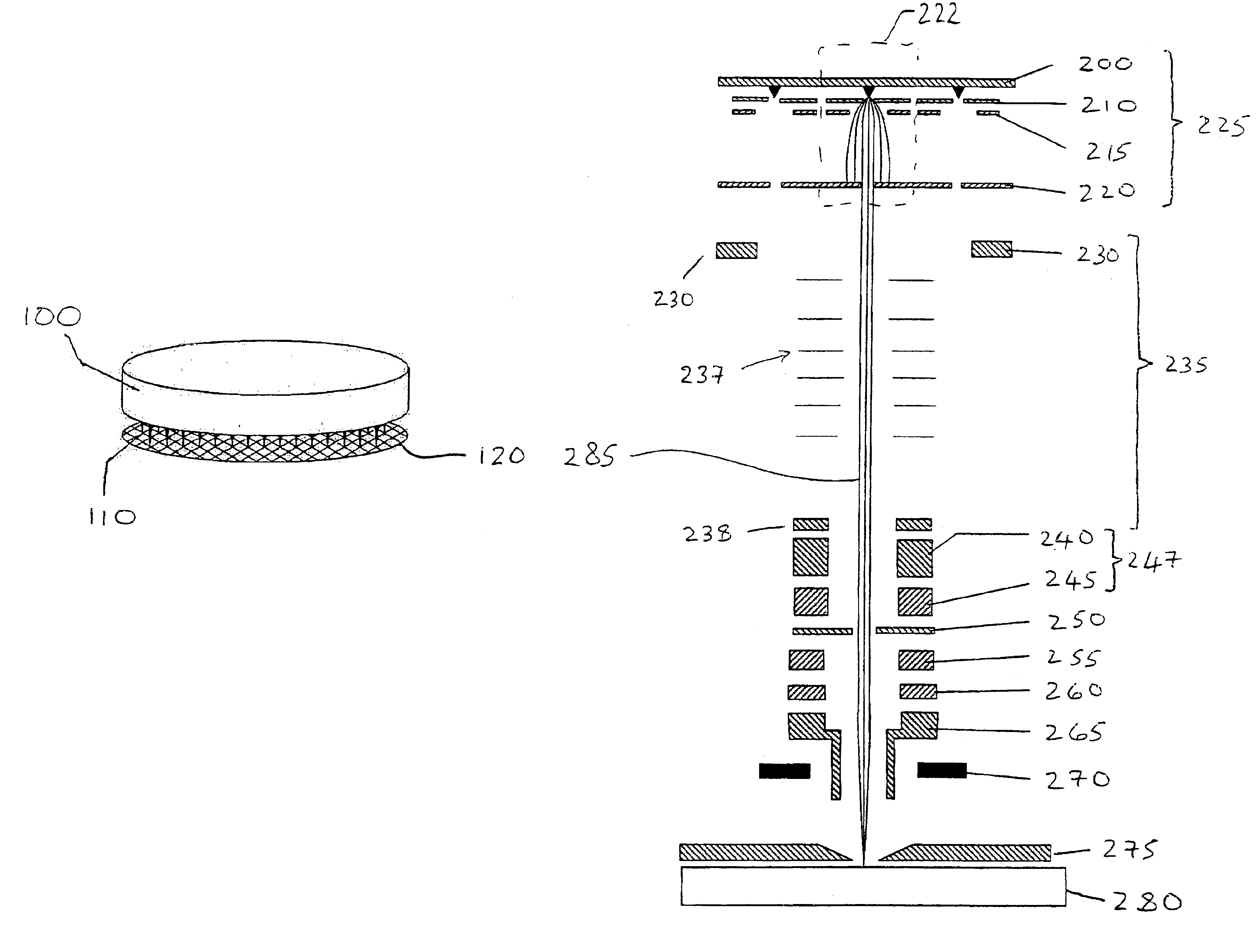
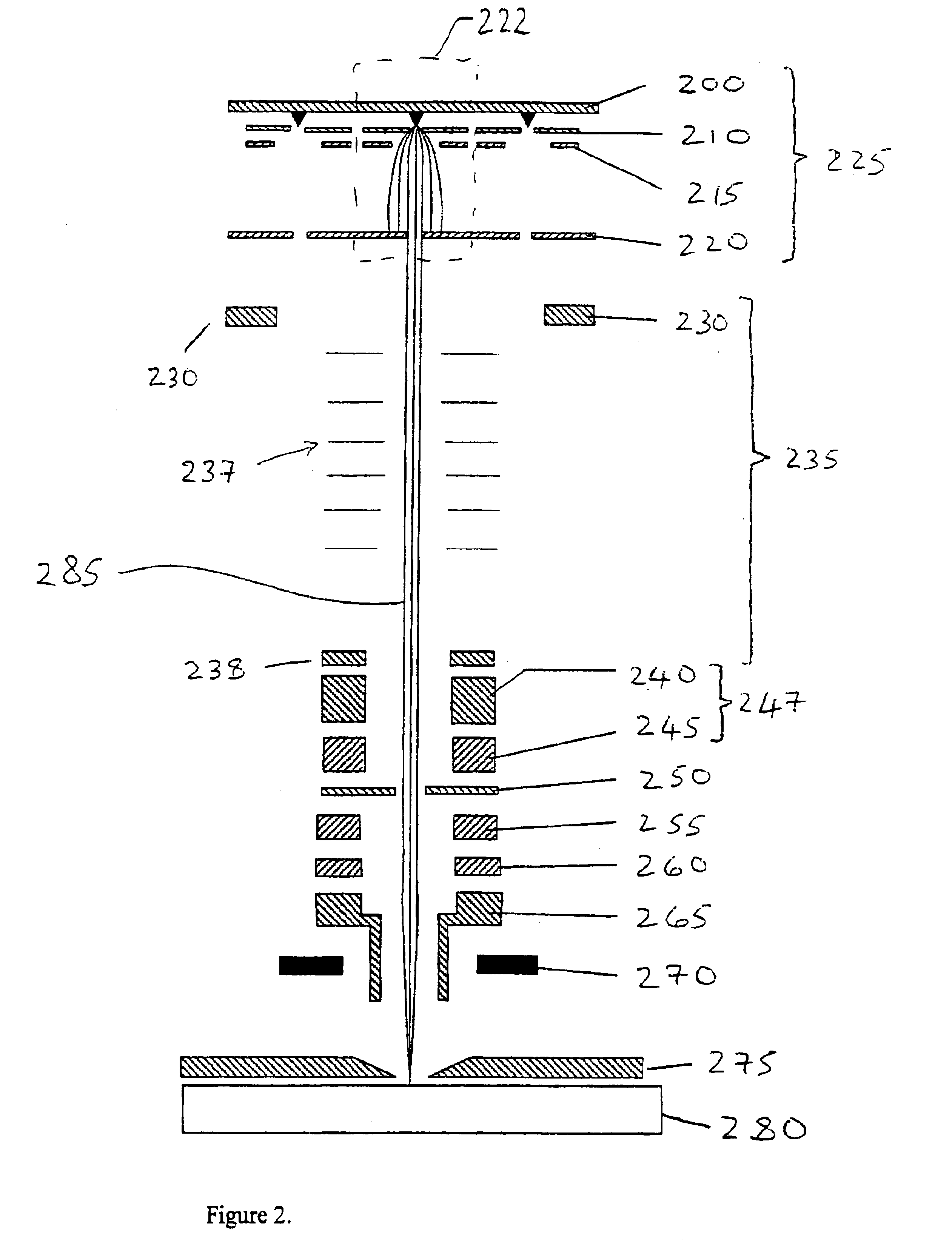
[0029]The invention disclosed herein is a high resolution electron beam wafer defect inspection tool that utilizes a multiple column, multiple source assembly to achieve wafer inspection at high throughput (suitable for in-line use in a semiconductor fabrication facility). The multiple columns allow for high throughput wafer inspection (up to several wafers per hour), and the multiple sources allow for both source redundancy, which will significantly decrease tool downtime and reduce service costs, and allow for more than one beam per column for advanced imaging. The tool is designed for the detection of defects for features with critical dimensions (CDs) in the range 25 nm-100 nm.

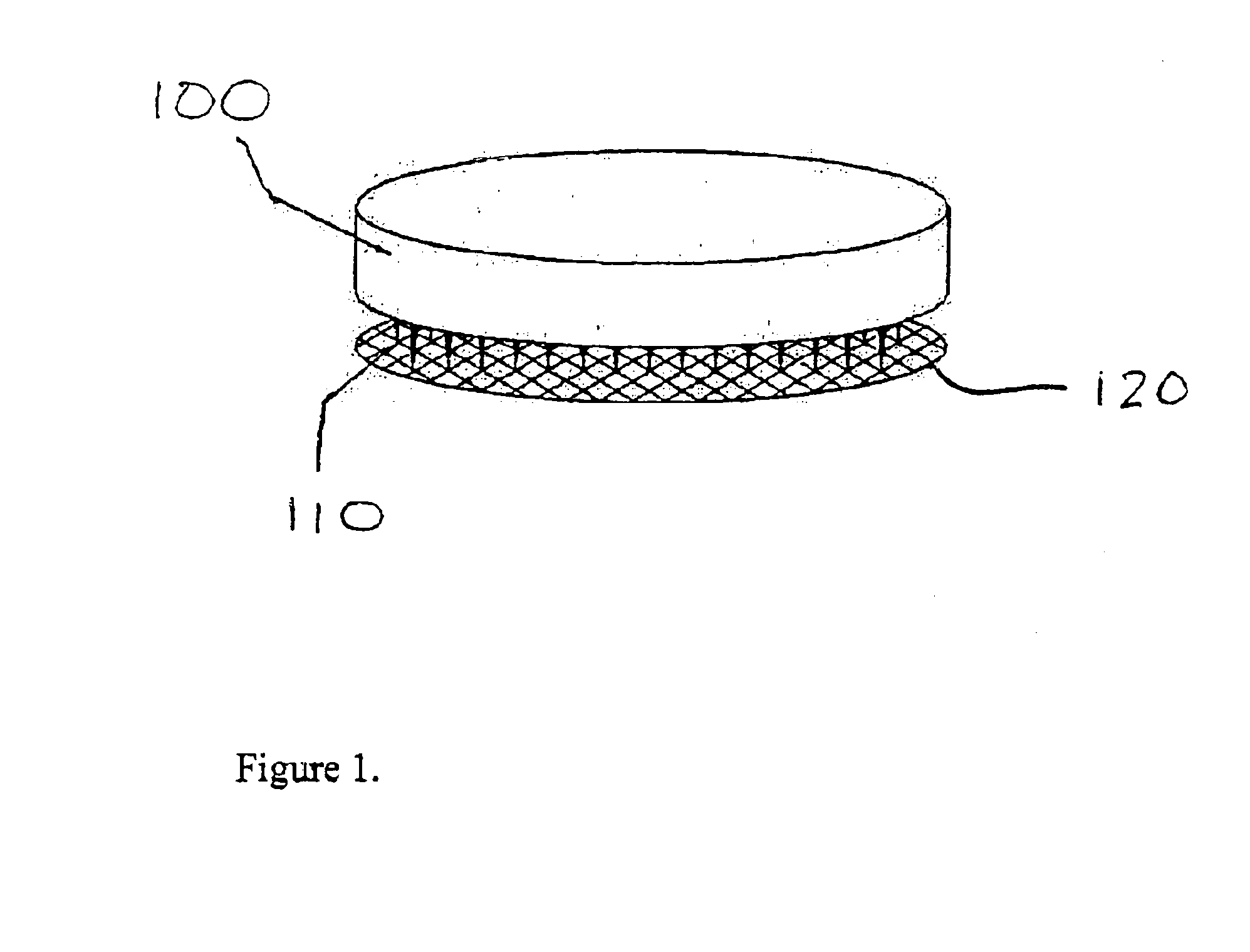
[0030]The electron beam inspection tool has multiple electron optical columns, each with its own electron source. There are no magnetic components in any of the columns—all of the focusing lenses and scanning deflectors are electrostatic. FIG. 1 shows a schematic of a multi-column assembly 100, positioned ...


PUM


Abstract

A multi-column electron beam inspection system is disclosed herein. The system is designed for electron beam inspection of semiconductor wafers with throughput high enough for in-line use. The system includes field emission electron sources, electrostatic electron optical columns, a wafer stage with six degrees of freedom of movement, and image storage and processing systems capable of handling multiple simultaneous image data streams. Each electron optical column is enhanced with an electron gun with redundant field emission sources, a voltage contrast plate to allow voltage contrast imaging of wafers, and an electron optical design for high efficiency secondary electron collection.

Description

CROSS-REFERENCE TO RELATED APPLICATIONS[0002]This application is a continuation of U.S. patent application Ser. No. 09 / 789,180 filed Feb. 19, 2001 now abandoned, which claims the benefit of U.S. Provisional Application No. 60 / 183,724 filed Feb. 19, 2000.BACKGROUND OF THE INVENTION[0003]1. Field of the Invention[0004]This invention relates to the field of wafer defect inspection, and in particular to wafer inspection using charged particle beams.[0005]2. Description of the Related Art[0006]Defect inspection of semiconductor wafers and masks for IC manufacturing is an accepted production process for yield enhancement. The information obtained from a wafer defect inspection tool can be used to flag defective dies for repair, or to improve wafer processing parameters. The systems used for inspection are typically optical in nature and such systems are limited in resolution due to the wavelength of the measuring light (200-400 nm). Although possible, it becomes increasingly difficult to ...

Claims


Application Information

Patent Timeline
IPC IPC(8): G21K1/00G21K1/087G21K5/10H01J37/28G01Q20/02G01Q30/02
CPCG21K1/087H01J37/28G21K5/10H01J2237/2817
Inventor YIN, EDWARD M.BRODIE, ALAN D.PARKER, N. WILLIAMTSAI, FRANK CHING-FENG
Owner MULTIBEAM CORP
Why Eureka
Try Eureka