Split-fabrication for light emitting display structures

a technology of light-emitting or organic electroluminescent displays and display structures, which is applied in the manufacture of electrode systems, electric discharge tubes/lamps, and discharge tubes luminescnet screens, etc., and can solve the problems of complex manufacturing process, low efficiency of structures, and limited options for driving display mediums

Inactive Publication Date: 2005-01-18
RUIZHANG TECH LTD CO
View PDF12 Cites 241 Cited by
  • Summary
  • Abstract
  • Description
  • Claims
  • Application Information

AI Technical Summary

Benefits of technology

FIGS. 9A to 9D illustrate a top view of a section of an active matrix display fabricated using the exemplary electroluminescent structures of the present invention and an exemplary advantage of the present invention in alignment of the two substrates (frontplane and backplane) together;
in alignment of the two substrates (frontplane and backplane) together;
FIG. 10A illustrates an exemplary tiled display fabricated according to some embodiments of the present invention; and
FIG. 10B illustrates an exemplary tiled display fabricated according to a current state of the art.

Problems solved by technology

Liquid crystal displays operate fairly reliably but their manufacturing process is complex and typically requires high power backlighting.
Although the relative positions of the anode and cathode layers 4 and 8 may be inverted, such structures yield devices with very low efficiency.
This limitation limits the options for driving the display medium, which in turn contributes to brightness nonuniformity typically seen in these types of active matrix displays.
When applying this configuration to making an OLED display, one problem with this configuration is that more complex planarization is required since the OLED display medium is usually too thin resulting in defects if the topography of the surface is not perfectly planarized.

Method used


Image

  • Split-fabrication for light emitting display structures
  • Split-fabrication for light emitting display structures
  • Split-fabrication for light emitting display structures

Examples


Embodiment Construction

In the following description, for purposes of explanation, numerous specific details are set forth in order to provide a thorough understanding of the present invention. It will also be appreciated that although the following examples relate to a making of a display, the present invention can be applied to a wide area of electronic devices without deviation from the merit of the invention. The following description and drawings are illustrative of the invention and are not to be construed as limiting the invention.

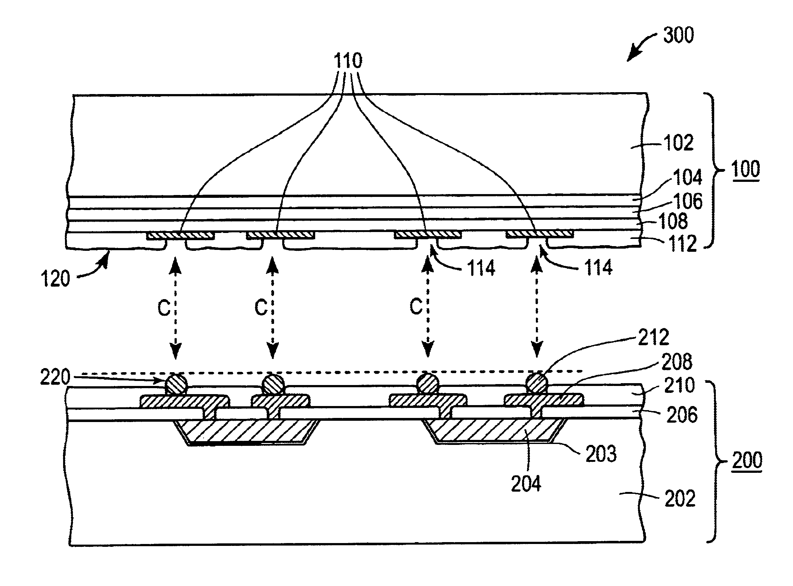
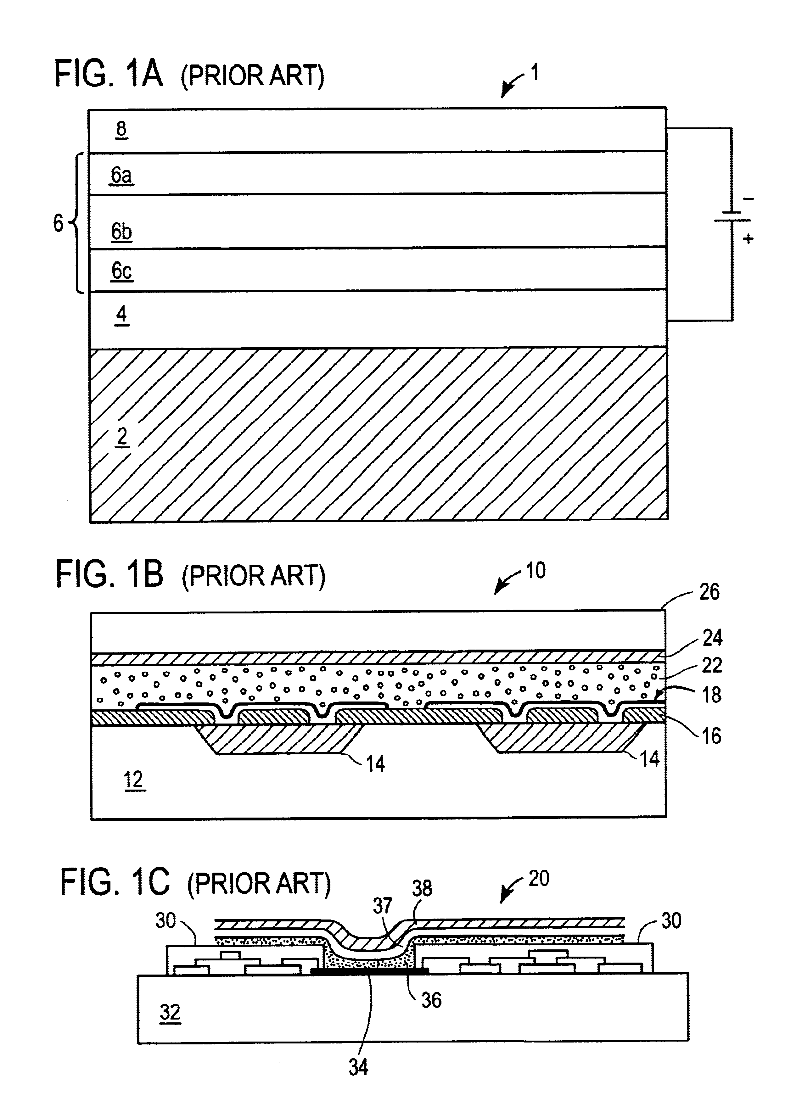
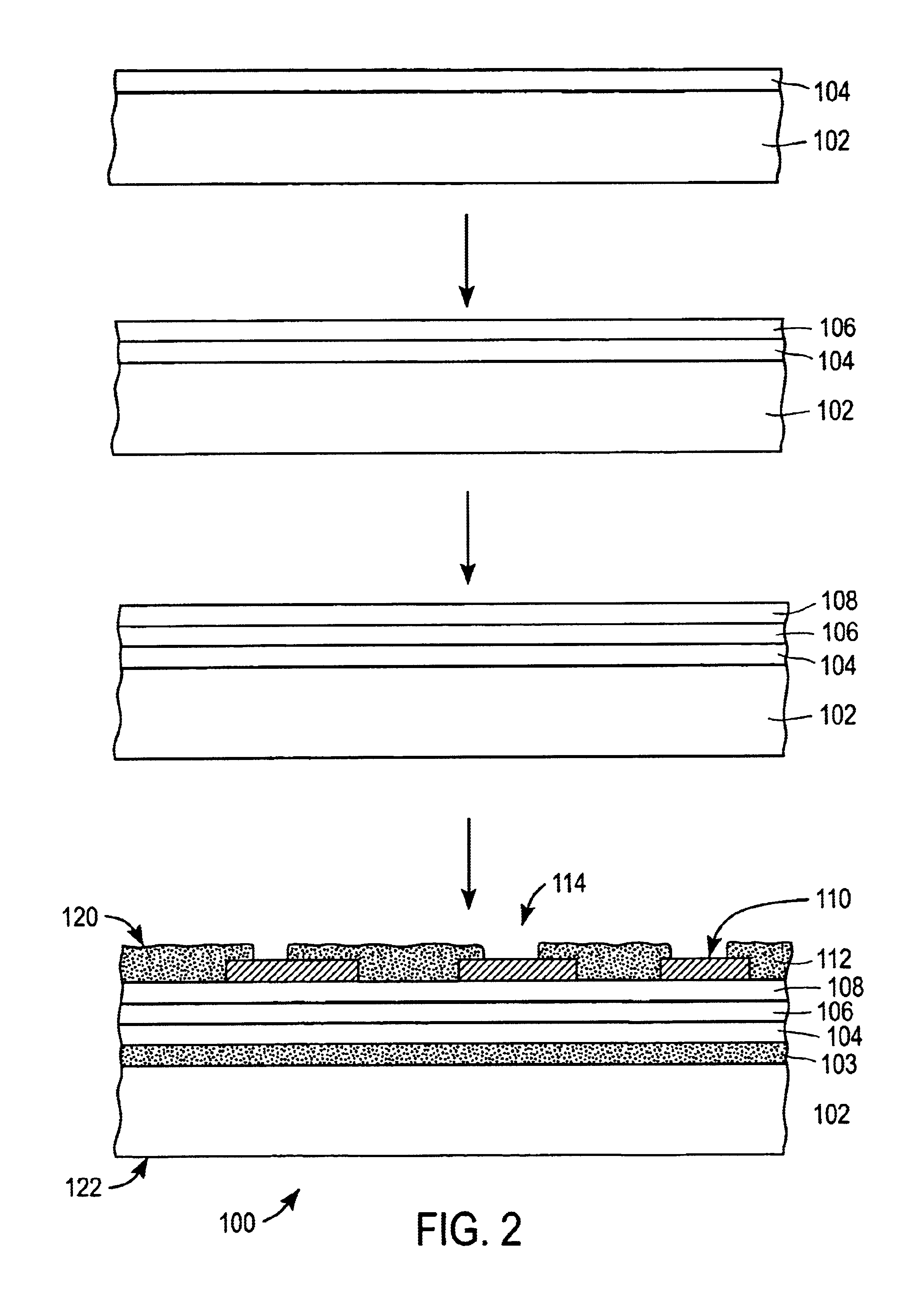
FIGS. 2 to 5 illustrate exemplary embodiments of the present invention with FIGS. 2 to 4 illustrate in details of how different layers of a display structure are laminated together. The display structure of the present invention includes an electroluminescent device that is a light emitting display structure. The electroluminescent device can be made out of an organic light emitting diode (OLED), or a polymer light emitting diode (PLED), also called a light emitting polyme...


PUM


Abstract

Methods and apparatuses for fabricating an electroluminescent display structure. A method including coupling a frontplane to a backplane wherein a frontplane top surface laminates to a backplane top surface. The frontplane and the backplane are fabricated separately. A first electrode layer which is transparent is disposed over the frontplane. A display medium which produces electro-optical effects upon a voltage application is disposed over the first electrode. A second electrode layer which is pattered is disposed over the display medium. The second electrode layer includes a plurality of connecting regions. The backplane is electrically active to provide driving signals for the display medium wherein the backplane includes a plurality of output pads to match the plurality of connecting regions.

Description

FIELD OF THE INVENTIONThe present invention relates generally to the field of fabricating flat panel displays (FPD). Specifically, the present invention relates to methods and apparatuses for split-fabrication of light emitting or organic electroluminescent displays and display structures.BACKGROUND OF THE INVENTIONFabrication of flat panel displays is well known in the art. Flat panel displays may be comprised of active matrix or passive matrix panels. Active matrix panels and passive matrix panels may be configured as transmissive, reflective, transflective or emissive dislays. Liquid crystals, electroluminescent (EL) materials, organic light emitting diodes (OLEDs), or light emitting diodes (LEDs), to name a few, may be used in fabricating flat panel displays. Liquid crystal displays operate fairly reliably but their manufacturing process is complex and typically requires high power backlighting. OLED are among the currently favored display types due to their promise to deliver f...

Claims


Application Information

Patent Timeline
Patent Type & Authority Patents(United States)
IPC IPC(8): H01J63/00H01J63/04H01J1/62H01J1/00H01L27/32
CPCH01L27/3253H01L24/95H01L2924/01012H01L27/3255H01L2224/95085H01L2224/95122H01L2224/95136H01L2924/0102H01L2924/01025H01L2924/01079H01L2924/09701H01L2924/14H01L2924/15155H01L2924/15165H01L2924/15311H01L2924/12041H01L2924/01084H01L2924/15153H01L2924/12044H10K59/1275H10K59/129H01L2924/00
Inventor BERNKOPF, JAN
Owner RUIZHANG TECH LTD CO
Why Eureka
Try Eureka