Organic light emitting didode display device having light-absorbing layer

a technology of light-absorbing layer and display device, which is applied in the direction of discharge tube luminescnet screen, discharge tube/lamp details, electric discharge lamps, etc., can solve the problems of affecting the recognition ability of organic light-emitting diode display device. , to achieve the effect of enhancing the recognition ability o

Inactive Publication Date: 2005-01-18
III HLDG 1
View PDF2 Cites 11 Cited by
  • Summary
  • Abstract
  • Description
  • Claims
  • Application Information

AI Technical Summary

Benefits of technology

An object of the present invention is to provide an organic light emitting diode display device having a light-absorbing layer to effectively reduce the amount of the reflected light, thereby raising the contrast ratio and enhancing the recognition ability of the display device.

Problems solved by technology

In other words, the recognition ability of a conventional organic light emitting diode display device becomes worse when the incident light is too strong.
The major drawbacks of the above structure are as follows: 1. It requires different equipment to form the organic functional layer and the transparent material layer.
The stress mismatch when using different equipment to form the organic functional layer and the transparent material layer would cause a higher err rate.
The organic functional layer would be damaged by the ion bombardment when forming the optical interference layer.
Sputtering process increases the costs for forming the optical interference layer because of higher costs of the sputtering equipment.

Method used


Image

  • Organic light emitting didode display device having light-absorbing layer
  • Organic light emitting didode display device having light-absorbing layer
  • Organic light emitting didode display device having light-absorbing layer

Examples


Embodiment Construction

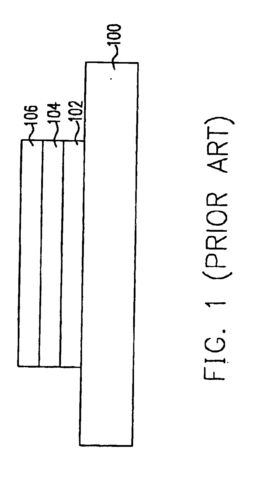
FIG. 3 shows the paths of incident light and the reflected light an organic light emitting diode display device. The organic light emitting diode display device comprises a transparent substrate 200, a plurality of strip transparent anodes 202 on the transparent substrate 200, an organic functional layer 204 on the transparent substrate 200, and a plurality of strip metal cathodes 206. The reflection rate n1 of the organic functional layer 204 is very close to the reflection rate n2 of the transparent anodes 202. The reflection rate n1 of the organic functional layer 204 is larger than the reflection rate n3 of the transparent substrate 200, wherein n1 is around 1.7, n2 is between 1.8-2.0, n3 is around 1.5, and n3 is larger than the reflection rate of air (around 1).

The light of the organic light emitting diode display device is generated by the organic functional layer 204. Although the direction of the light is ransom, the light can transmit toward the transparent substrate 200 be...


PUM


Abstract

The present invention provides an organic light emitting diode display device, having a transparent substrate; a plurality of anodes on the transparent substrate; an organic functional layer on the transparent substrate, wherein the transparent substrate covers the anodes; a light-absorbing layer on the organic functional layer, wherein the light-absorbing layer is an organic material layer and the organic material layer is doped with at least a metal; and a plurality of cathodes on the light-absorbing layer. The light-absorbing layer of the present invention can effectively reduce the amount of the reflected light, thereby raising the contrast ratio and enhancing the recognition ability of the display device.

Description

CROSS REFERENCE TO RELATED APPLICATIONSThis application claims the priority benefit of Taiwan application Ser. no. 91112772, filed on Jun. 12, 2002.BACKGROUND OF INVENTION1. Field of the InventionThis invention generally relates to an organic light emitting diode display device, and more particularly to an organic light emitting diode display device having a light-absorbing layer.2. Description of Related ArtFlat panels haven been widely used in communication industries as interfaces between the users and the machines such as portable communication products. Some major flat panel technologies are plasma display, liquid crystal display, electro-luminescent display, light emitting display and electro-chromic display. However, compared to those flat panel technologies, organic light emitting diode (“OLED”) has advantages of self-emitting, less power consumption, low costs, low temperature operation, high response speed, and no viewing angle dependence. Hence, it is highly potential tha...

Claims


Application Information

Patent Timeline
Patent Type & Authority Patents(United States)
IPC IPC(8): H01L51/50H01L51/52H01L27/32H01L27/28
CPCH01L51/5281H01L27/3281H10K59/17H10K50/86
Inventor CHANG, MEI-YINGLIAO, CHI-CHIHLEE, JIUN-HAW
Owner III HLDG 1
Why Eureka
Try Eureka