

Fast PDLC device
- Summary
- Abstract
- Description
- Claims
- Application Information
AI Technical Summary
Benefits of technology
Problems solved by technology
Method used
Image

Examples
Embodiment Construction
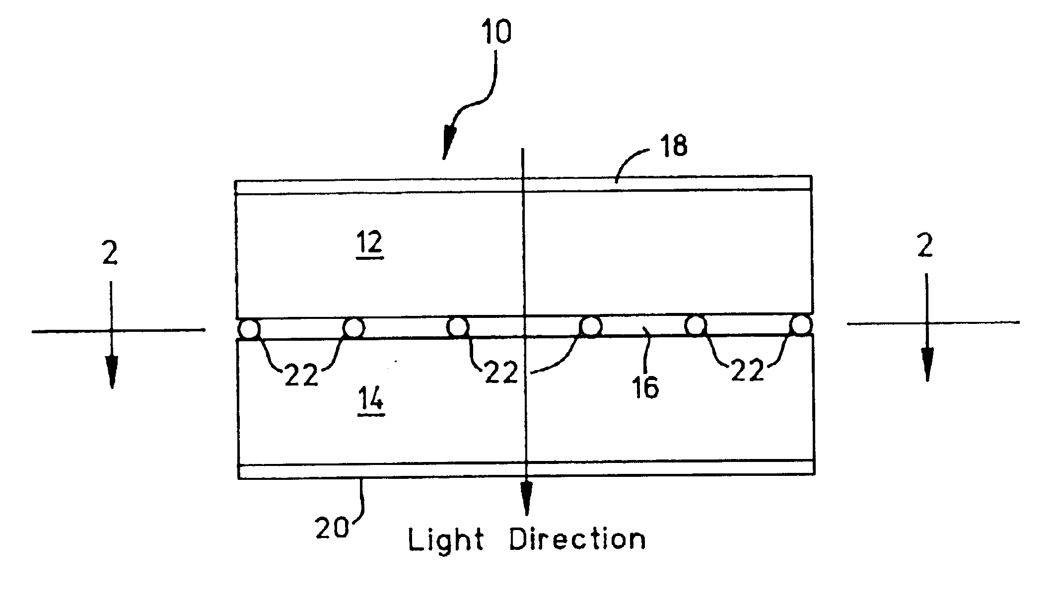
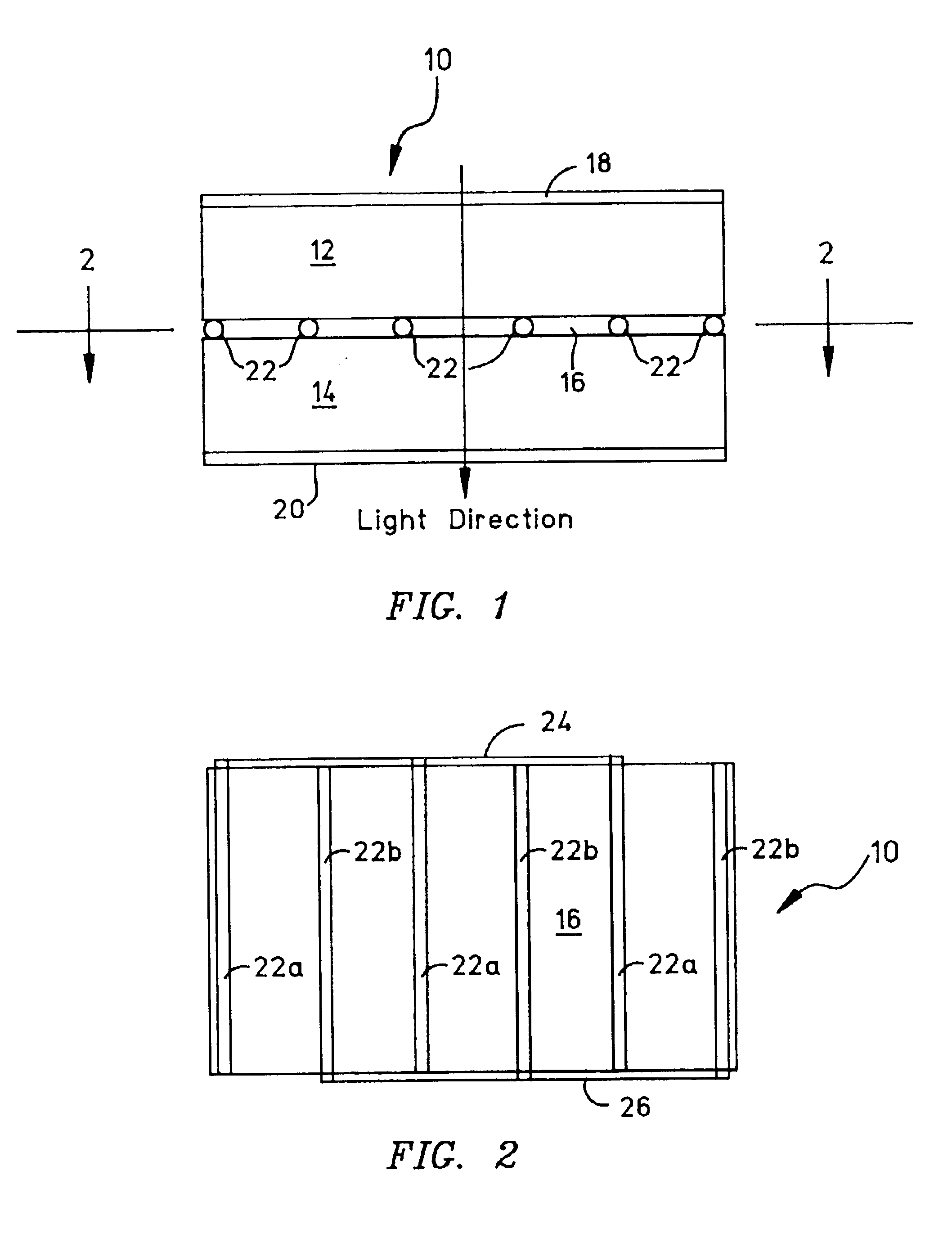
Referring to FIG. 1, in accordance with the present invention a PDLC device 10 includes a first non-conductive substrate 12 and a second non-conductive substrate 14 spaced closely parallel to the first substrate 12 so that an interior surface of the first substrate 12 opposes an interior surface of the second substrate 14. At least one of the substrates is made of a transparent material such as suitable glass or plastic. More particularly, where the device 10 is intended for use in a display device operating in a reflection mode, only one of the substrates is transparent. Where the device 10 is intended to be used as a pass through window, such as an optical modulator, both substrates 12 and 14 must be transparent. By way of example, the substrates 12 and 14 could be made of transparent polyester sheet material having a thickness of approximately 0.008 inches.
A generally planar layer 16 of a conventional PDLC material is sandwiched between a pair of interior surfaces of the first an...
PUM
| Property | Measurement | Unit |
|---|---|---|
| Thickness | aaaaa | aaaaa |
| Electrical conductivity | aaaaa | aaaaa |
| Diameter | aaaaa | aaaaa |
Abstract
Description
Claims
Application Information