Semiconductor memory device

a memory device and semiconductor technology, applied in semiconductor devices, digital storage, instruments, etc., can solve the problems of large area of memory cells, liable to loose information of memory cells of one-transistor and one-capacitor structures, etc., and achieve high data holding stability

Inactive Publication Date: 2005-01-18
RENESAS ELECTRONICS CORP
View PDF8 Cites 9 Cited by
  • Summary
  • Abstract
  • Description
  • Claims
  • Application Information

AI Technical Summary

Benefits of technology

An object of the invention is to provide a semiconductor memory device using memory cells, which have structures not increasing areas, and are arranged in a distinctive manner providing high data holding stability.
According to the above structure, the memory cell of the two-transistor and one-capacitor type can be formed in a small region through steps prepared only by making a simple change to conventional steps of manufacturing the semiconductor memory device. In the process of manufacturing an integrated circuit of the memory array, the memory cells can be arranged at a high density without making a significant change to the conventional steps of manufacturing the semiconductor memory device. As a result, the semiconductor memory device, which has good data holding stability, has a high-density structure and exhibits high yield, can be manufactured at a low cost.

Problems solved by technology

A memory cell of one-transistor and one-capacitor structure is liable to loose its information, and particularly, data at a high potential level (H-data) due to leak of electric charges stored in the capacitor.
However, the above method requires two transistors and two capacitors, and therefore suffers from such a problem that areas of the memory cells are large.

Method used


Image

  • Semiconductor memory device
  • Semiconductor memory device
  • Semiconductor memory device

Examples


first embodiment

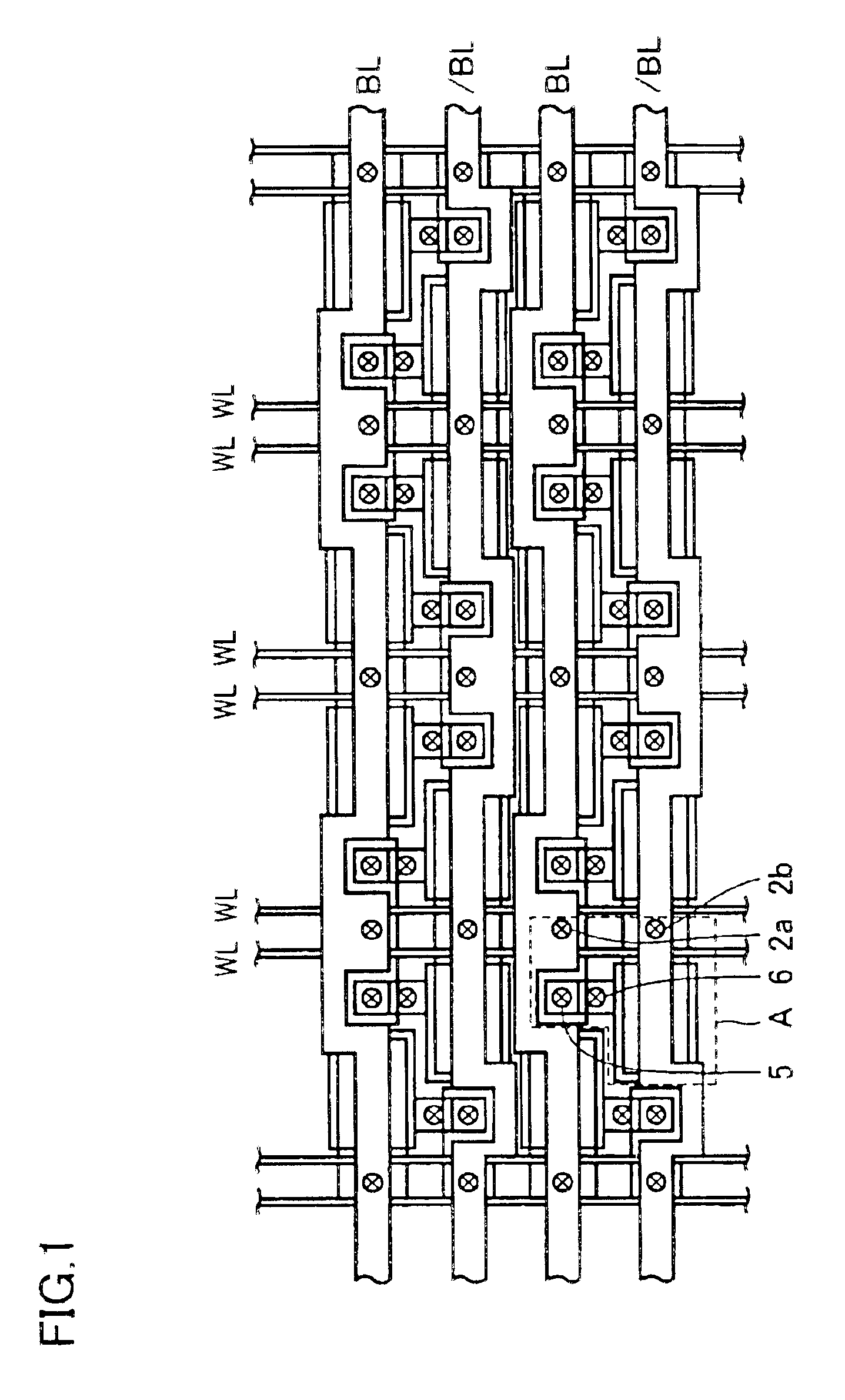
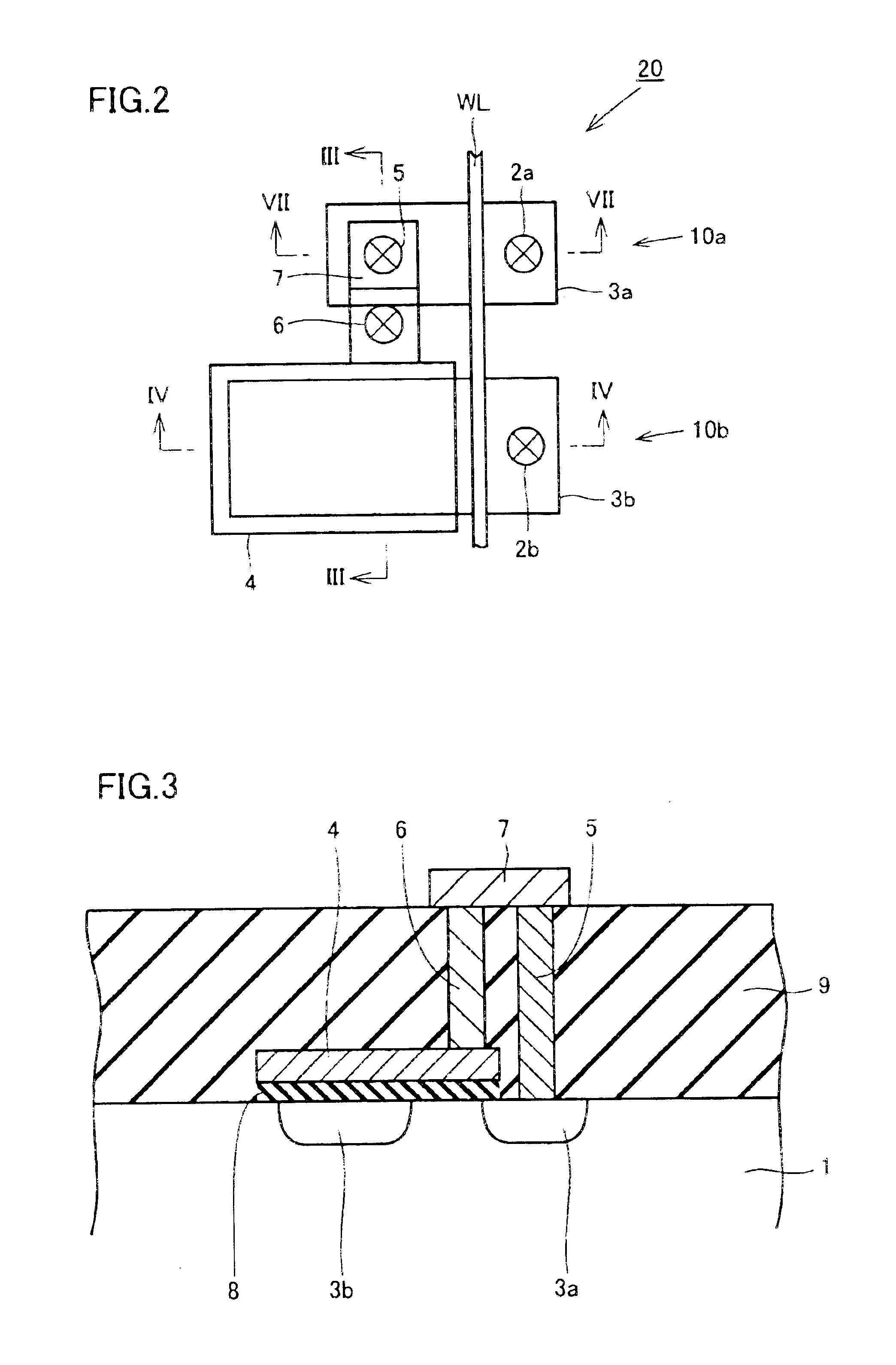
FIG. 1 shows an arrangement in a DRAM of a first embodiment of the invention. In FIG. 1, a memory cell in the DRAM is formed of two transistors and one capacitor. This DRAM can be achieved by repeating an arrangement of a portion, which is the memory cell including the two transistors and the one capacitor, and is indicated by “A”, by parallel translation, mirror-image mapping or point-symmetrical mapping. In FIG. 1, bit line contacts 2a and 2b are located under bit lines BL and / BL, respectively. Plug interconnections 5 and 6 form contacts for connecting the two transistors to an electrode of the capacitor.

FIG. 2 shows, on an enlarged scale, the portion indicated by “A” in FIG. 1. In this portion, two MOS transistors 10a and 10b are arranged along a word line WL serving also as gate electrodes. MOS transistors 10a and 10b have impurity regions 3a and 3b, respectively. The capacitor which is commonly used by the two transistors is formed between a cell plate 4 and impurity region 3b ...

second embodiment

A memory cell of a second embodiment of the invention differs from that of the first embodiment in that both the two transistors are connected only to the storage node side, and neither of them is connected to the cell plate.

In FIG. 14, the memory cells of the two-transistor and one-capacitor type of the invention are arranged to form a storage device of the background refresh type. In the semiconductor memory device of the background refresh type, one of the two transistors forming the memory cell is utilized as the access transistor, and the other is utilized as the transistor for refresh. In the array arrangement shown in FIG. 14, the memory cells of the two-transistor and one-capacitor type are present in a portion indicated by “C”, and this portion C is shown, on an enlarged scale, in FIG. 15. FIG. 16 is a cross section taken along line XVI—XVI in FIG. 15.

In FIG. 16, one transistor 10a has impurity region 3a connected to an access bit line ABL via bit line contact 2a as well as...

third embodiment

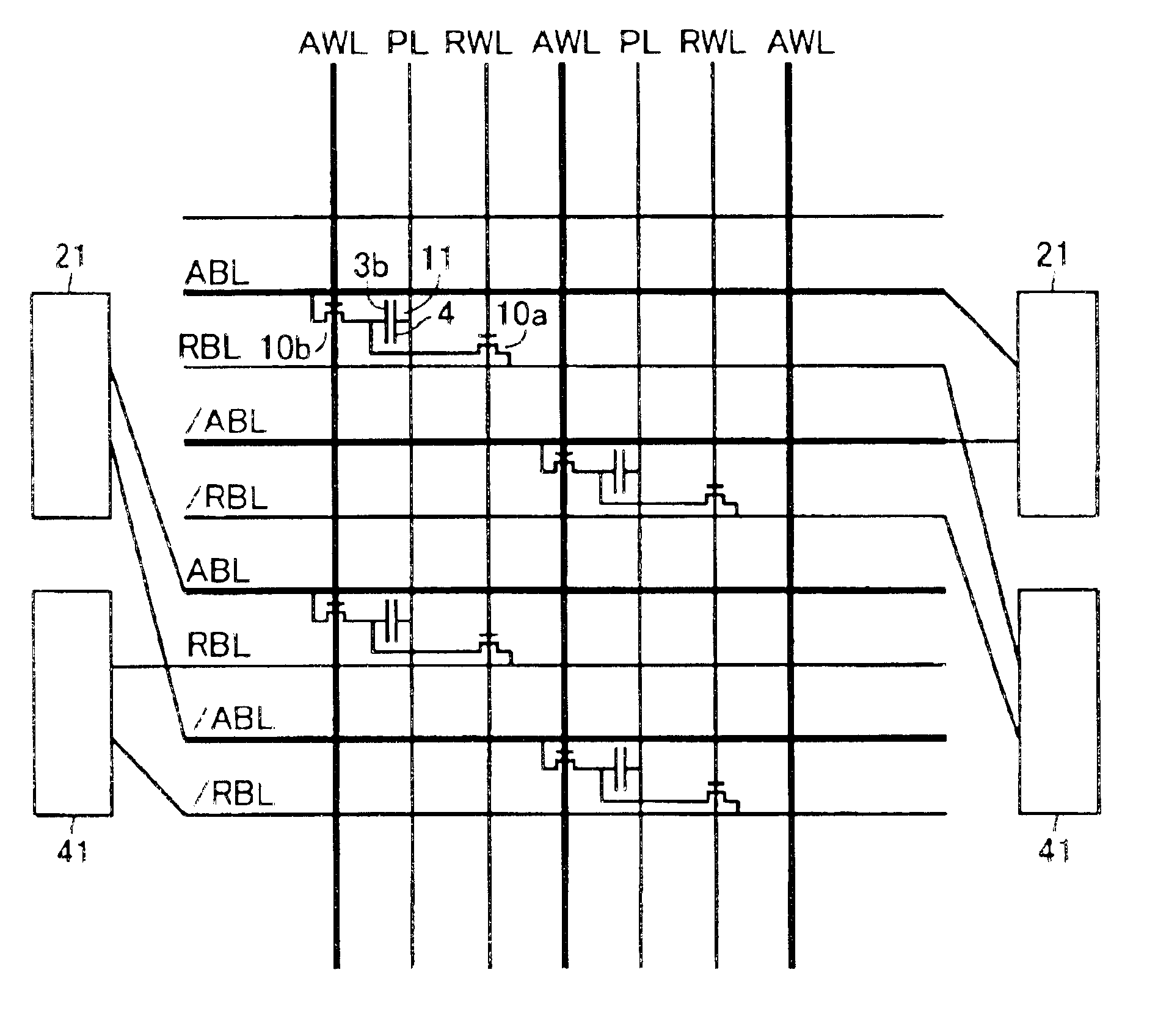
FIG. 21 shows a connection structure of sense amplifiers in a DRAM of the complementary capacity type of a third embodiment of the invention. The memory cell is of the two-transistor and one-capacitor type, and is the same as that of the second embodiment. However, the DRAM of this embodiment is of the complementary capacity type. Therefore, the two memory cells of the two-transistor and one-capacitor type in the second embodiment are coupled together to form one memory cell pair of this embodiment. Further, one of the transistors is used for the normal access, and the other is used for the refresh. This structure is the same as that in the arrangement of the second embodiment.

In the DRAM of the complementary capacity type described above, two memory cells are used for writing H-data and L-data, respectively. For this, the sense amplifiers and the bit lines are connected in such a manner that one access sense amplifier is connected to two access bit lines or two complementary access...


PUM


Abstract

A semiconductor memory device uses memory cells, which have structures not increasing areas, and are arranged in a distinctive manner providing high data holding stability.A semiconductor memory device includes memory cells formed on a main surface of a semiconductor substrate, and each having first and second transistors each having a gate electrode and impurity regions forming source / drain as well as one capacitor; and bit and word lines for controlling an operation of the memory cells, a cell plate forming an electrode of the capacitor being formed of the same layer as the gate electrode.

Description

BACKGROUND OF THE INVENTION1. Field of the InventionThe present invention relates to a semiconductor memory device, and particularly relates to a semiconductor memory device including memory cells, which have specific or distinctive structures, as well as a semiconductor memory device having a memory cell array, which has a specific or distinctive structure.2. Description of the Background ArtA memory cell of one-transistor and one-capacitor structure is liable to loose its information, and particularly, data at a high potential level (H-data) due to leak of electric charges stored in the capacitor. In recent years, such a method has been proposed that uses two memory cells for writing H-data and L-data (i.e., data at a lower potential than Hdata) therein, respectively. This method is devised to utilize a difference in amount of stored electric charges between the two memory cells, and thereby provide a Dynamic Random Access Memory (DRAM) performing a larger operation.However, the a...

Claims


Application Information

Patent Timeline
Patent Type & Authority Patents(United States)
IPC IPC(8): G11C11/405G11C5/06G11C11/4097G11C11/409G11C11/403H01L27/108G11C11/401G11C11/404G11C11/406H01L21/8242
CPCG11C5/063G11C11/405H01L27/108G11C11/4097H01L27/10897H10B12/00H10B12/50
Inventor OOISHI, TSUKASA
Owner RENESAS ELECTRONICS CORP
Why Eureka
Try Eureka