
Encapsulated optoelectronic devices with controlled properties

a technology of optoelectronic devices and controlled properties, applied in the direction of semiconductor laser structure details, semiconductor lasers, optical resonator shape and construction, etc., can solve problems such as inaccurate prior testing, and achieve the effect of reducing the amount of transmission increas

Inactive Publication Date: 2005-01-18
OPTICAL COMM PRODS
View PDF32 Cites 30 Cited by
  • Summary
  • Abstract
  • Description
  • Claims
  • Application Information

AI Technical Summary

Problems solved by technology

Optical feedback provided by the cleaved mirrors creates a resonance of the emitted light that results in lasing.
If the facet transmission changes after encapsulation, however, the slope efficiency and threshold current will change, making the prior testing inaccurate.

Method used


Image

  • Encapsulated optoelectronic devices with controlled properties
  • Encapsulated optoelectronic devices with controlled properties
  • Encapsulated optoelectronic devices with controlled properties

Examples


Embodiment Construction

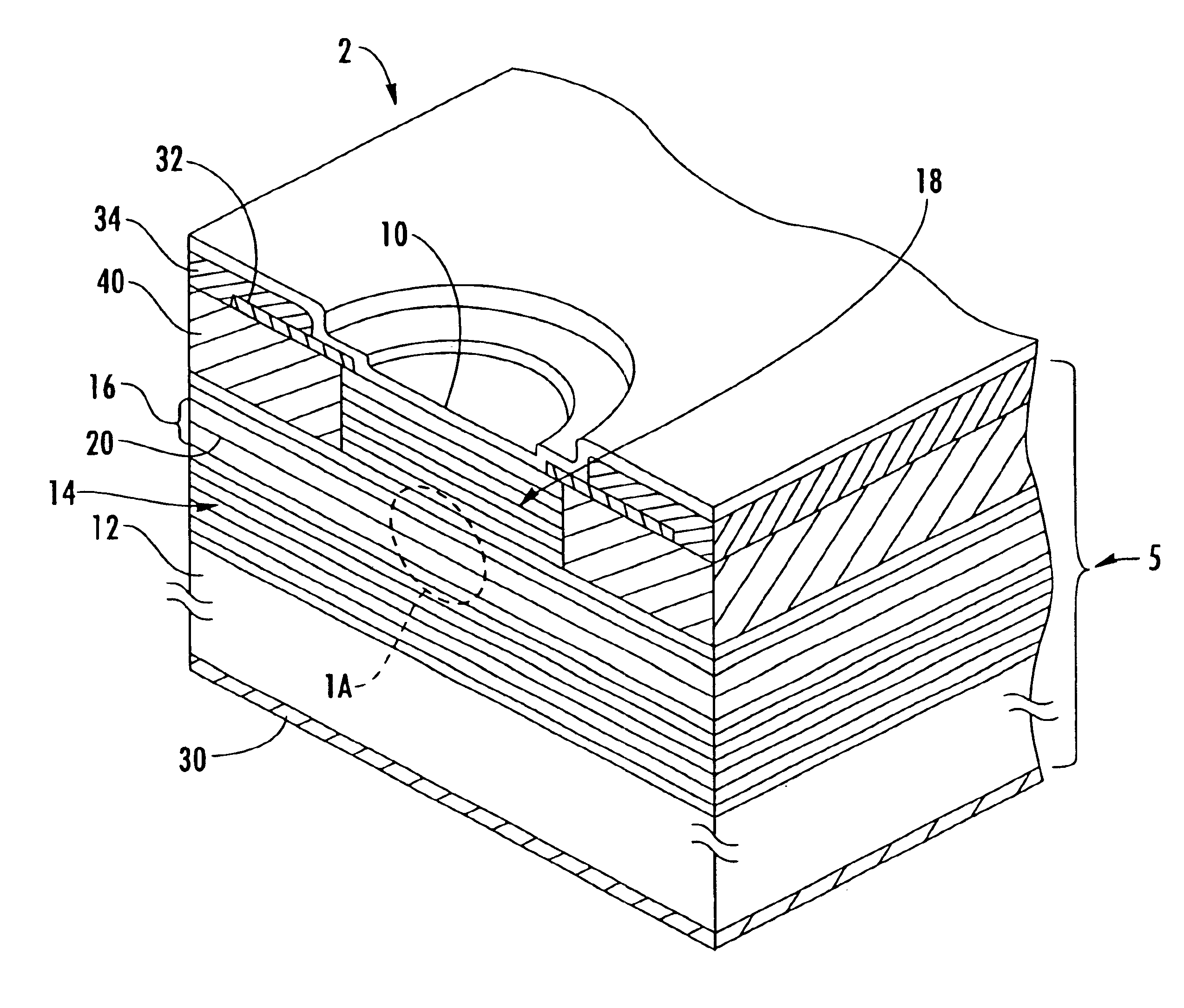
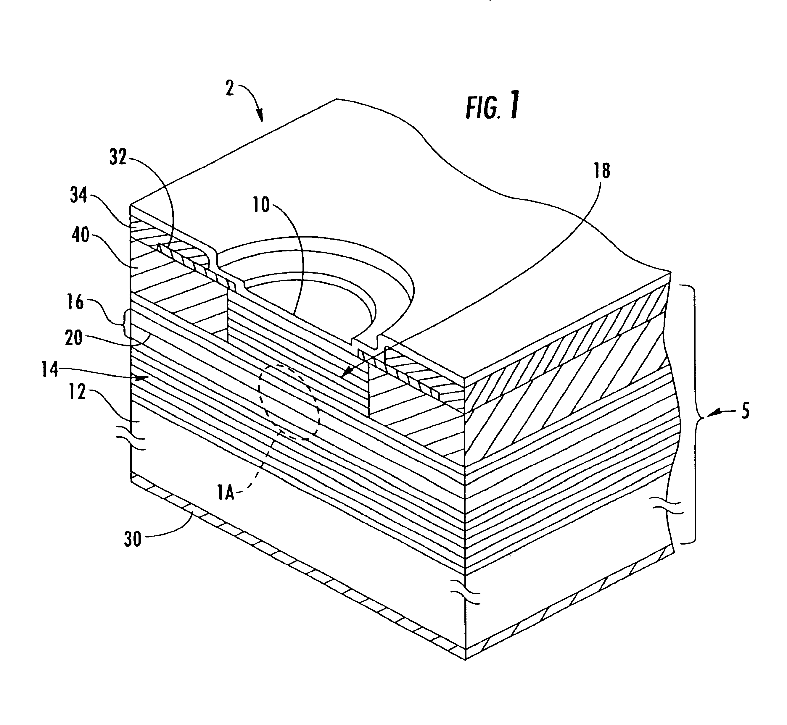
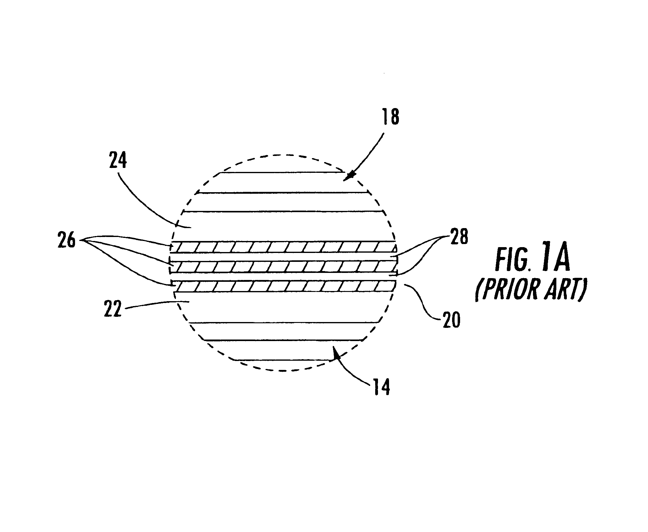
The present invention provides a design for an optoelectronic device such as a VCSEL whose transmission does not change upon encapsulation by a material such as plastic, epoxy or other suitable encapsulant with a known index of refraction. FIGS. 21 and 21A are qualitative graphical representations of the characteristics of two lasers pre and post encapsulation. The plot in FIG. 21 is from a laser fabricated conventionally illustrating how characteristics of the device change after encapsulation. The plot in FIG. 21A, made from a laser fabricated according to the present invention, illustrates how the characteristics of the device are controlled and remain substantially the same after encapsulation. In one embodiment of the invention, the optoelectronic device is a conventional VCSEL or a VCSEL with a variable tuning layer that enables growth of wafers of VCSELs with consistent properties. In the following description, the VCSEL with variable tuning layer is presented first, followed...


PUM


Abstract

An optoelectronic device, such as a VCSEL, is disclosed whose transmission does not change upon encapsulation by a material such as plastic, epoxy or other suitable encapsulant with a known index of refraction. The surface reflection of the VCSEL surface is very different depending on whether it is terminated in air or the encapsulant, with a much larger reflection in the case of air. It is known that the surface reflection can be made out of phase with the rest of the mirror, effectively increasing the transmission. The amount of the transmission increase can be adjusted by controlling the thickness of the surface layer. Once the VCSEL is encapsulated, the surface reflection is reduced, and the transmission at the facet is increased but the dephased reflection is also reduced. Depositing a surface layer whose index of refraction is similar to the encapsulant, and adjusting the surface layer thickness correctly, the overall transmission from the laser into the terminating material is unchanged, be it air or encapsulation. As a result, the laser properties such as slope efficiency and threshold current are unchanged upon encapsulation. The same procedure may be applied to devices other than VCSELs such as other types of lasers, LEDs, and resonant cavity photodetectors to achieve encapsulated optoelectronic components with controlled properties that remain unchanged upon encapsulation.

Description

FIELD OF THE INVENTIONThe invention relates to the field of optical devices, and more particularly, to an apparatus and method for controlling the properties of optoelectronic components encapsulated by a material with an index of refraction substantially different from air.BACKGROUNDSemiconductor lasers are widely used in applications such as optical communications. The edge emitting laser diode is a semiconductor laser that emits light from a plane which is a continuation of the p-n junction of the diode. Cleaved surfaces at the ends of the diode act as mirrors which together define an optical cavity. Optical feedback provided by the cleaved mirrors creates a resonance of the emitted light that results in lasing.The vertical cavity surface emitting laser (VCSEL) is another type of semiconductor laser in which the optical cavity is normal to the p-n junction of the semiconductor wafer from which it was fabricated. Ordinarily VCSELs are manufactured with many layers of semiconductor...

Claims


Application Information

Patent Timeline
Patent Type & Authority Patents(United States)
IPC IPC(8): H01L33/00H01S5/022H01S5/00H01S5/183H01S5/02H01S5/028H01L33/10H01L33/44H01L33/46
CPCH01L33/44H01S5/02284H01S5/18391H01L33/105H01L2224/48091H01L33/465H01S5/0042H01S5/0201H01S5/02228H01S5/02296H01S5/0264H01S5/18369H01S5/18377H01L2924/00014H01S5/02234H01S5/02251H01S5/02257
Inventor SCOTT, JEFFREY W.
Owner OPTICAL COMM PRODS
Learn More