Method of forming cutting elements

a technology of semi-conductive polycrystalline diamond and cutting element, which is applied in the field of polycrystalline diamond, can solve the problems of reducing the flexibility of being able to provide pcd coating, brittleness also increases, and the hardness of pcd material hardness, wear resistance and thermal stability, etc., and achieves enhanced cuttability and increased conductivity of the semi-conductive pcd material of the present invention

Inactive Publication Date: 2005-01-25
SMITH INT INC
View PDF6 Cites 46 Cited by
  • Summary
  • Abstract
  • Description
  • Claims
  • Application Information

AI Technical Summary

Benefits of technology

According to either of the exemplary methods of formation, the ultra hard PCD layer is formed as a semiconductor material with increased conductivity compared to PCD layers formed of conventional insulative diamond crystals, such as Type I di

Problems solved by technology

While a higher metal binder content typically increases the toughness of the resulting PCD material, higher metal content also decreases the PCD material hardness, wear resistance and thermal stability.
Thus, these inversely affected desired properties ultimately limit the flexibility of being able to provide PCD coatings having desired levels of both wear resistance and toughness to meet the service demands of particular applications.
Additionally, when the PCD composition is chosen to increase the wear resistance of the PCD material, typically brittleness also increases, thereby reducing the toughness o

Method used


Image

  • Method of forming cutting elements
  • Method of forming cutting elements
  • Method of forming cutting elements

Examples


Embodiment Construction

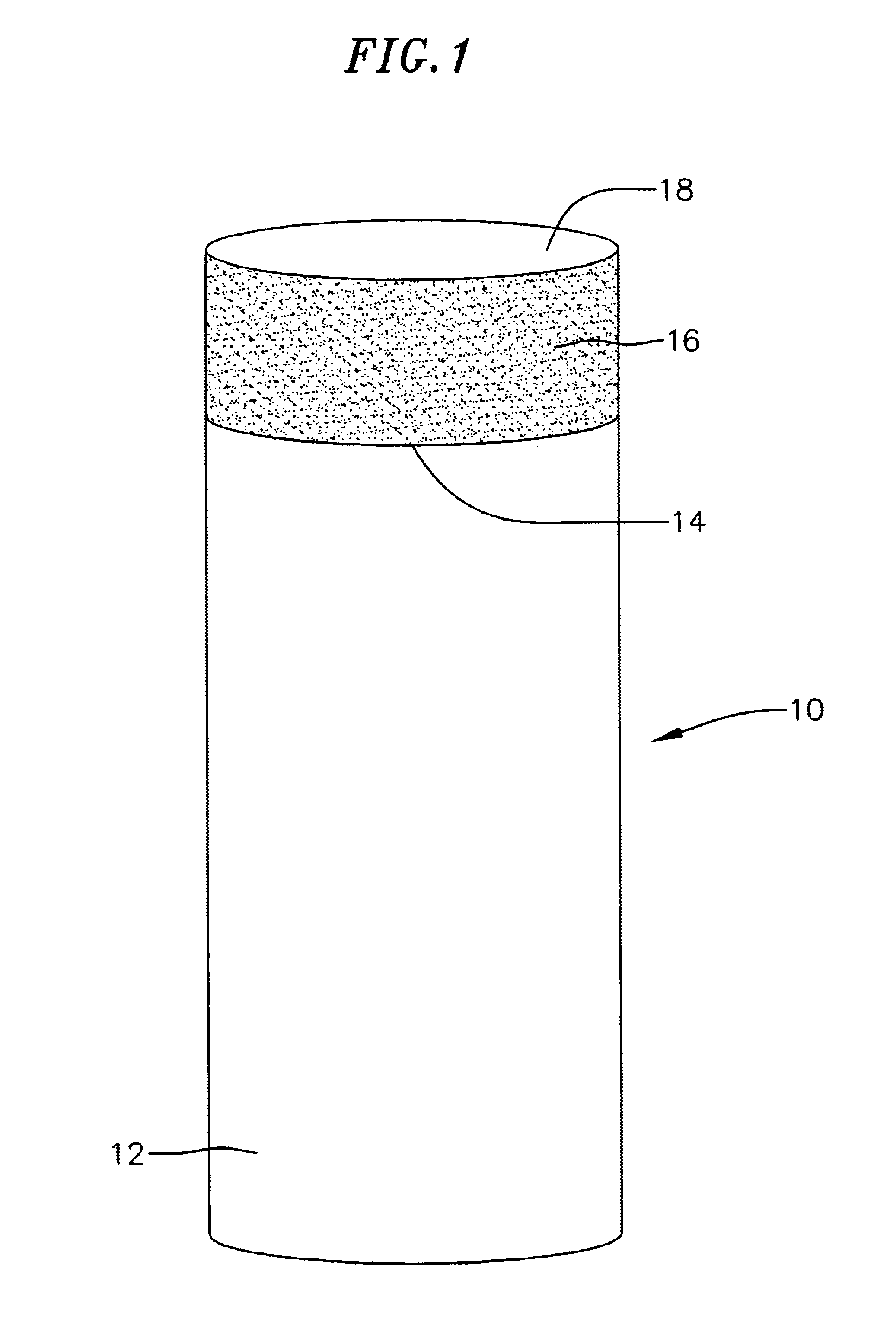
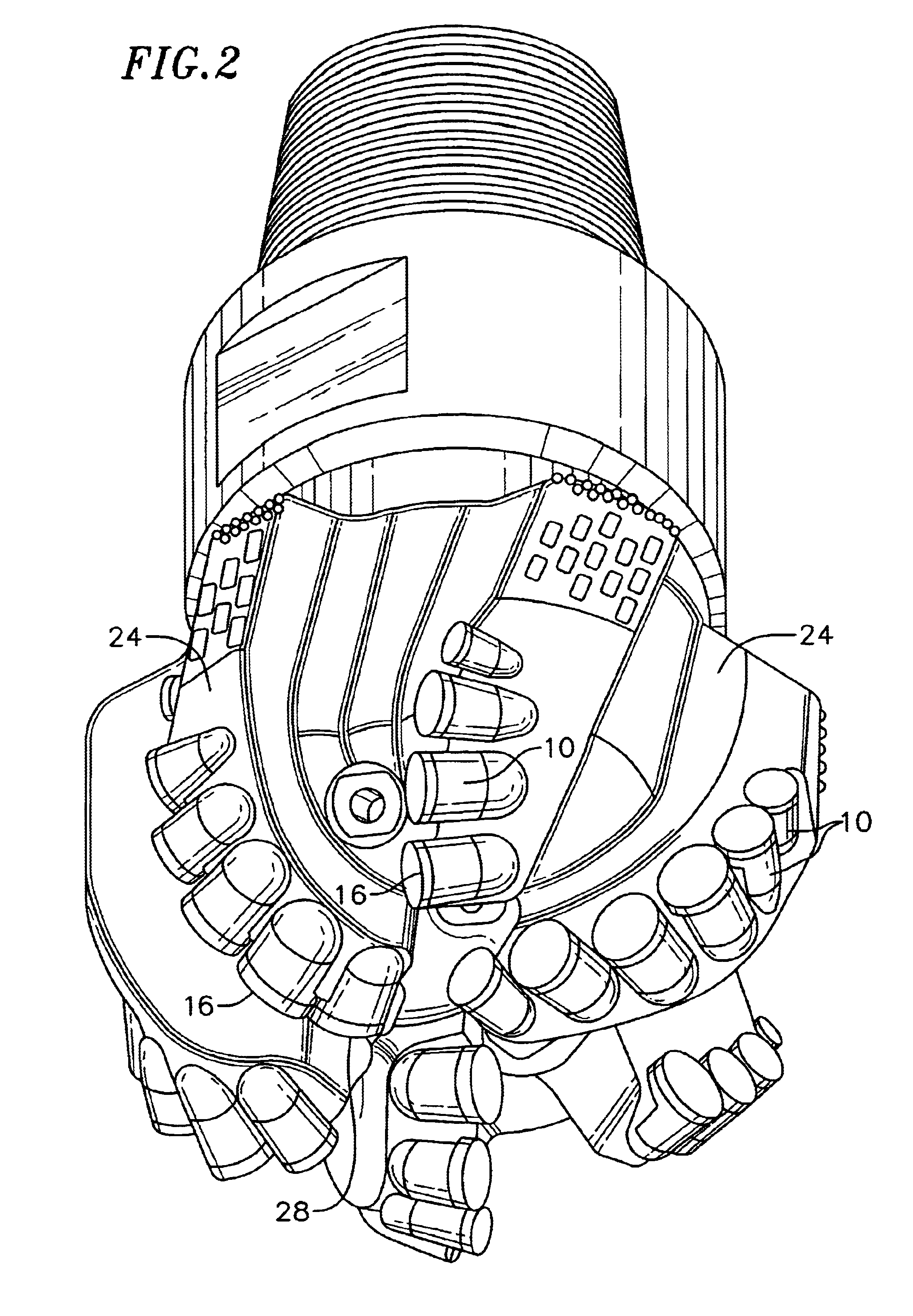
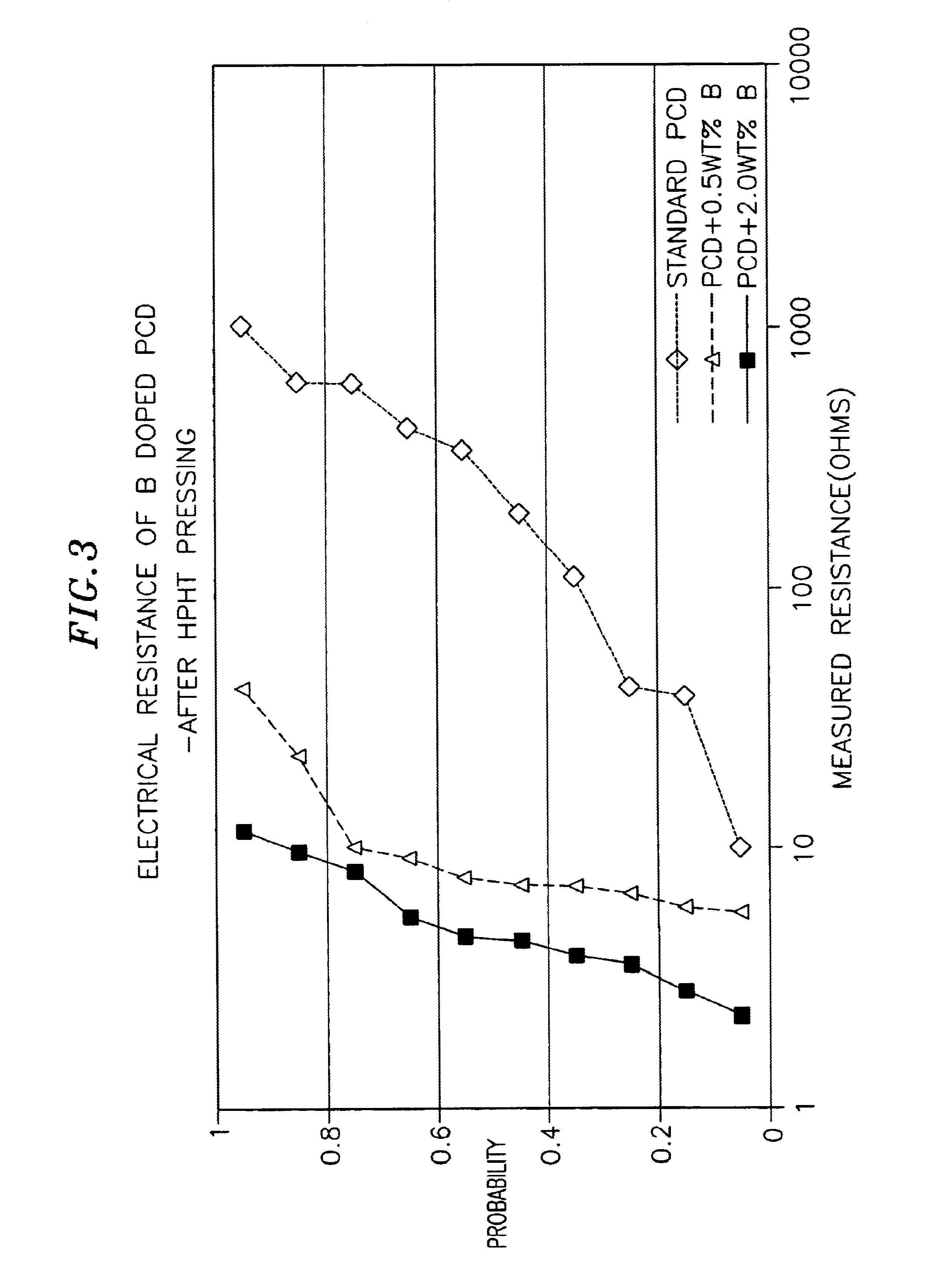
A PCD material having enhanced cuttability, especially EDM and EDG cuttability without comprising its hardness, wear resistance, or thermal stability, cutting and other tools incorporating such material, and a method of making such material and tools, are provided. An exemplary embodiment PCD material of the present invention has a substantial percentage of diamond crystals that are semiconductive in nature or which include semiconductive outer surface layers. Such diamond crystals contain small quantities of interstitial impurities such as lithium (Li), beryllium (Be), boron (B), and aluminum (Al) that are sufficient to make them semiconductors.

Semiconductive diamonds are discussed in Wentorf, R. H. and Bovenkirk, H. P., “Preparation of Semiconducting Diamonds,” J. Chem. Phys. 36, p. 1987 (1962); Field, J. E., “Properties of Diamond,” Academic Press, 1979; and, Wentorf, R. H., “Diamond Formation at High Pressures”, in Advances in High Pressure Research, Academic Press, p.249-281 (1...


PUM

PropertyMeasurementUnit
Fractionaaaaaaaaaa
Electrical resistanceaaaaaaaaaa

Abstract

An ultra-hard semiconductive polycrystalline diamond (PCD) material formed with semiconductive diamond particles doped with Li, Be or Al and/or insulative diamond particles having semiconductive surfaces, tools incorporating the same, and methods for forming the same, are provided. The ultra-hard PCD material may be formed using a layer of insulative diamond grit feedstock that includes additives therein, then sintering to convert a plurality of the diamond crystals to include a semiconductive surface. In another embodiment, the ultra-hard PCD material is formed by sintering semiconductive diamond grit feedstock consisting of diamond crystals doped with Li, Al or Be. The ultra-hard semiconductive PCD cutting layer exhibits increased cuttability, especially in EDM and EDG cutting operations.

Description

BACKGROUND OF THE INVENTIONThis invention relates to polycrystalline diamond and more specifically to semiconductive polycrystalline diamond that exhibits enhanced cuttability, especially Electro-Discharge Machining or Electro-Discharge Grinding cuttability.Polycrystalline diamond (PCD) materials known in the art are typically formed from diamond grains or crystals and a ductile metal catalyst / binder, and are synthesized by high temperature / high pressure (“HTHP”) processes. Such PCD materials are ultra hard materials well known for their mechanical property of high wear resistance, making them a popular material choice for use in such industrial applications as cutting tools for machining, and subterranean mining and drilling, where the mechanical property of wear resistance is highly desired. In such applications, conventional PCD materials can be provided in the form of a surface coating, e.g., on inserts used with cutting and drilling tools, to improve wear resistance of the inse...

Claims


Application Information

Patent Timeline
IPC IPC(8): B22F7/06C23C30/00C23C24/08C23C24/00B23B51/00B22F3/10B23B27/14B23B27/20B23P15/28C04B35/52
CPCB22F7/06C04B35/52C23C30/005C23C24/08B22F2005/001C04B2235/40C04B2235/402C04B2235/405C04B2235/421C04B2235/427C04B2235/96C04B2235/404
Inventor MIDDLEMISS, STEWART
Owner SMITH INT INC
Why Eureka
Try Eureka