Vertical-cavity surface-emitting semiconductor laser

a semiconductor laser and vertical cavity technology, applied in semiconductor lasers, laser details, optical resonator shape and construction, etc., can solve the problems of unstable operation, above-described structure not achieving optical constriction, etc., to achieve dynamic stability, small element volume, and high speed modulation characteristics

Inactive Publication Date: 2005-01-25
NIPPON TELEGRAPH & TELEPHONE CORP
View PDF12 Cites 0 Cited by
  • Summary
  • Abstract
  • Description
  • Claims
  • Application Information

AI Technical Summary

Benefits of technology

[0009]A first object of the present invention is to provide a vertical-cavity surface-emitting semiconductor laser which provides single transverse mode operation that is dynamically stable as compared with a conventional vertical-cavity surface-emitting semiconductor laser.
[0010]A second object of the present invention is to provide a vertical-cavity surface-emitting semiconductor laser having a smaller element volume than a conventional vertical-cavity surface-emitting semiconductor laser which provides high speed modulation characteristics and provides single transverse mode operation that is dynamically stable as compared with a conventional vertical-cavity surface-emitting semiconductor laser.
[0012]A fourth object of the present invention is to provide a process for fabricating a vertical-cavity surface-emitting semiconductor laser having a smaller element volume than a conventional vertical-cavity surface-emitting semiconductor laser which provides high speed modulation characteristics and provides single transverse mode operation that is dynamically stable as compared with a conventional vertical-cavity surface-emitting semiconductor laser.

Problems solved by technology

However, the above-described structures do not achieve optical constriction due to refractive index optical waveguide but are of an anti-guide waveguide structure.
However, in dynamic characteristics in which the carrier density inside the active layer varies widely, there arises the problem that an unstable operation occurs, that is, higher order modes may emerge depending on the carrier density distribution in the active layer.

Method used


Image

  • Vertical-cavity surface-emitting semiconductor laser
  • Vertical-cavity surface-emitting semiconductor laser
  • Vertical-cavity surface-emitting semiconductor laser

Examples


first embodiment

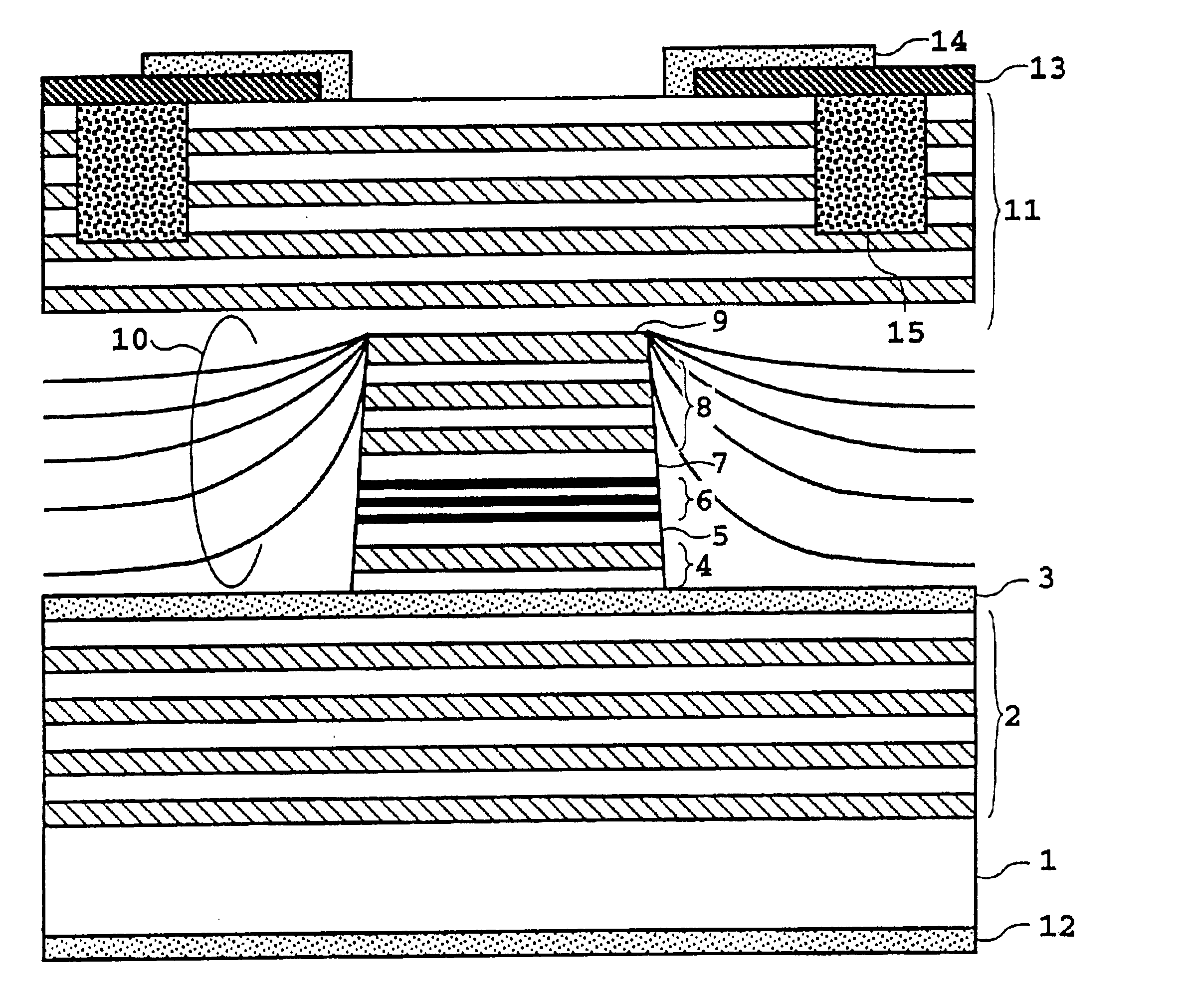
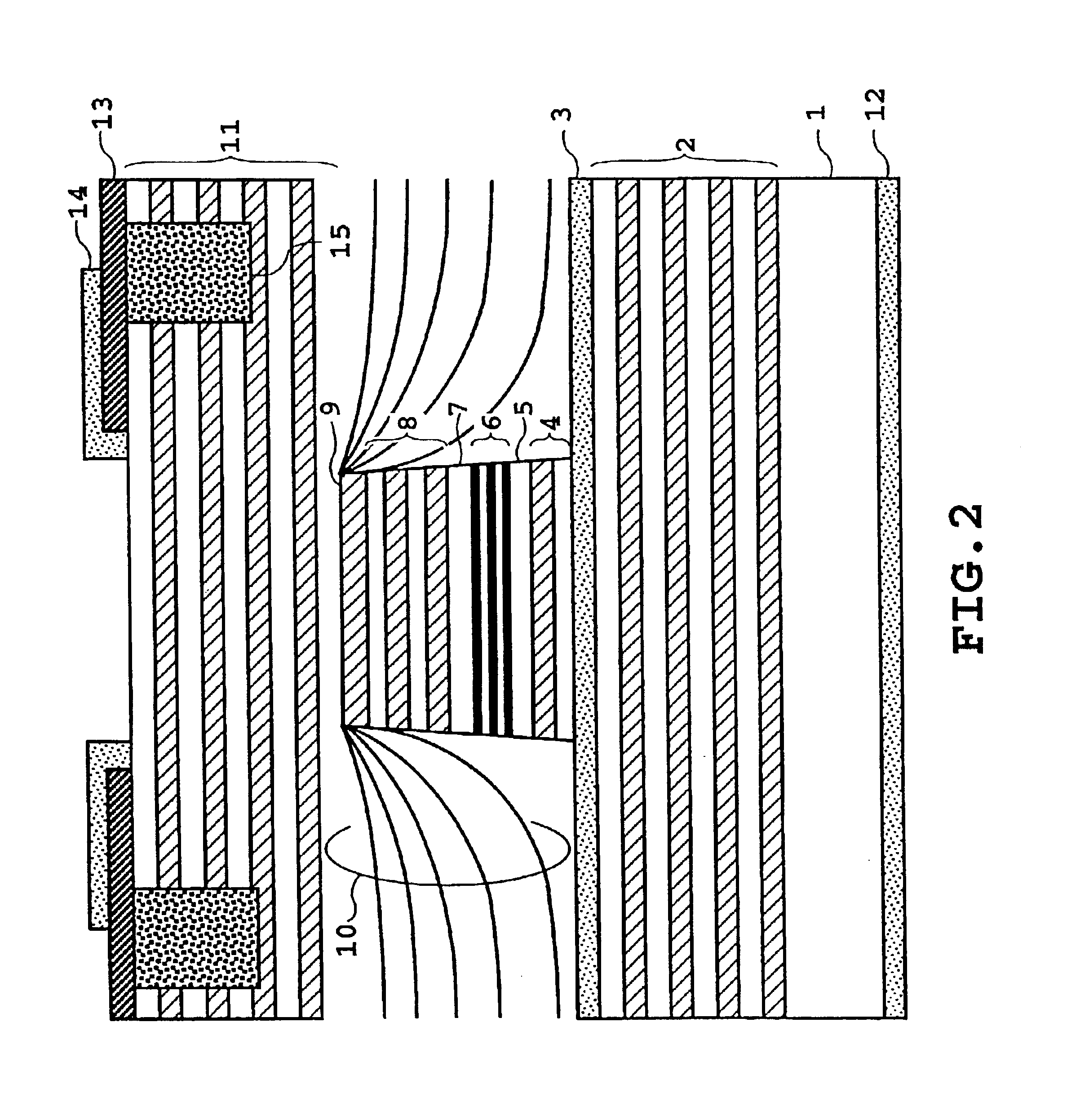
[0025]FIG. 2 is a cross-sectional view of a vertical-cavity surface-emitting semiconductor laser element according to a first embodiment of the present invention along the direction vertical to a face of crystal growth. This structure includes a p-GaAs substrate 1, which has thereon in order a p-AlyGa1-yAs / AlzGa1-zAs (02 (the dashed portion showing AlzGa1-zAs and the white or non-dashed portion showing AlyGa1-yAs), a p-InGaP etch stop layer 3, a p-AlyGa1-yAs / AluGa1-uAs (04 (the dashed portion showing AluGa1-uAs and the white or non-dashed portion showing AlyGa1-yAs), a non-doped AlwGa1-wAs lower spacer layer 5, a GaAs / AlxGa1-xAs multiple quantum well (MQW) active layer 6, a non-doped AlwGa1-wAs upper spacer layer 7, an n-AlyGa1-yAs / AluGa1-uAs (08 (the dashed portion showing AluGa1-uAs and the white or non-dashed portion showing AlyGa1-yAs), an n-InGaP first growth final layer 9, an AlGaAs or InGaP semiconductor buried layer (second growth layer) 10, an n-AlyGa1-yAs / AlzGa1-zAs (011, ...

second embodiment

[0033]FIG. 6 is a cross-sectional view showing a vertical-cavity surface-emitting semiconductor laser element according to the instant embodiment along the direction vertical to a plane of crystal growth. This structure includes a p-GaAs substrate 1, which has thereon in order a p-AlyGa1-yAs / AlzGa1-zAs (02 (the dashed portion showing AlzGa1-zAs and the white or non-dashed portion showing n-AlyGa1-yAs), a p-InGaP etch stop layer 3, a p-AlyGa1-yAs / AluGa1-uAs (04 (the dashed portion showing AluGa1-uAs and the white or non dashed portion showing AlyGa1-yAs), a non-doped AlwGa1-wAs lower spacer layer 5, a GaAs / AlxGa1-xAs (06, a non-doped AlwGa1-wAs upper spacer layer 7, an n-AlyGa1-yAs / AluGa1-uAs (08 (the dashed portion showing AluGa1-uAs and the white or non-dashed portion showing)AlyGa1-yAs, an n-AlyGa1-yAs / AlzGa1-zAs (09,an AlGaAs or InGaP semiconductor buried layer 10, a lower electrode 11, an insulator 12, an upper electrode 13, and an element separating structure 14. Of the above-d...

third embodiment

[0038]FIG. 8 is a cross-sectional view showing a vertical-cavity surface-emitting semiconductor laser element according to the instant embodiment along the direction vertical to a plane of crystal growth. This structure includes a p-GaAs substrate 1, which has thereon in order a p-AlyGa1-yAs / AlzGa1-zAs (02 (the dashed portion showing AlzGa1-zAs and the white or non-dashed portion showing AlyGa1-yAs), a p-InGaP etch stop layer 3, a p-AlyGa1-yAs / AluGa1-uAs (04 (the dashed portion showing AlzGa1-zAs and the white or non-dashed portion showing AlyGa1-yAs), a non-doped AlwGa1-wAs lower spacer layer 5, a GaAs / AlxGa1-xAs multiple quantum well (MQW) active layer 6, a non-doped AlwGa1-wAs upper spacer layer 7, an n-AlyGa1-yAs / AluGa1-uAs (08, an n-InGaP last layer 9 in first growth, an AlGaAs or InGaP semiconductor buried layer (second growth layer) 10, an n-AlyGa1-yAs / AlzGa1-zAs (011, a lower electrode 12, an insulator 13, an upper electrode 14, and an element separating structure 15. The re...


PUM


Abstract

A vertical-cavity surface-emitting semiconductor laser has a substrate, a lower DBR structure portion having a plurality of layers provided on the substrate, a semiconductor buried structure portion provided over the lower DBR structure portion having at least one layer with buried therein an active layer, and an upper DBR structure portion having a plurality of layers provided over the semiconductor buried structure portion including the active layer. The active layer, at least one layer arranged over the active layer and at least one layer arranged beneath the active layer constitute an optical resonator region and each of the layers constituting the optical resonator region has an effective refractive index higher than respective effective refractive indices of other layers in the upper and lower DBR structure portions and a refractive index of the at least one layer constituting the semiconductor buried structure portion.

Description

[0002]This is a divisional of application Ser. No. 09 / 261,465 filed Feb. 24, 1999 now U.S. Pat. No. 6,549,553.BACKGROUND OF THE INVENTION[0003]1. Field of the Invention[0004]The present invention relates to a process for fabricating a vertical-cavity surface-emitting semiconductor laser, which is useful as an optical source for optical interconnection that optically connects chips or boards to each other or for conducting two-dimensional parallel signal processing, and to a vertical-cavity surface-emitting semiconductor laser.[0005]2. Description of the Related Art[0006]Vertical-cavity surface-emitting semiconductor lasers, which are easy to construct a two-dimensional array and enables high efficient coupling with fibers without use of lenses for coupling because of their illumination pattern being circular, are considered important as an optical source for optical interconnection or two-dimensional parallel signal processing and also important for the purpose of reducing power con...

Claims


Application Information

Patent Timeline
Patent Type & Authority Patents(United States)
IPC IPC(8): H01S5/00H01S5/183H01S5/227
CPCH01S5/18308H01S5/18347H01S5/209H01S2301/166H01S5/2222H01S5/2224H01S5/222
Inventor UENOHARA, HIROYUKITATENO, KOUTAKAGAWA, TOSHIAKITADANAGA, OSAMUAMANO, CHIKARAKUROKAWA, TAKASHI
Owner NIPPON TELEGRAPH & TELEPHONE CORP
Why Eureka
Try Eureka