System and method to form a composite film stack utilizing sequential deposition techniques

a composite film and sequential deposition technology, applied in the direction of chemical vapor deposition coating, semiconductor/solid-state device details, coatings, etc., can solve the problems of affecting the operation of the resulting electrical circuit, affecting the thermal and electrical conductivity of the resulting contact, and attempting to provide interconnect materials with lower electrical resistivity

Inactive Publication Date: 2005-02-01
APPLIED MATERIALS INC
View PDF203 Cites 59 Cited by
  • Summary
  • Abstract
  • Description
  • Claims
  • Application Information

AI Technical Summary

Problems solved by technology

Formation of contacts in multi-level integrated circuits poses many challenges to the semiconductor industry as the drive to increase circuit density continues, due to the reduction in size of the circuit features.
In addition, diffusion between the aluminum and the surrounding insulating material often occurs, which adversely effects operation of the resulting electrical circuits.
Otherwise, the thermal and electrical conductance of the resulti...

Method used


Image

  • System and method to form a composite film stack utilizing sequential deposition techniques
  • System and method to form a composite film stack utilizing sequential deposition techniques
  • System and method to form a composite film stack utilizing sequential deposition techniques

Examples


Embodiment Construction

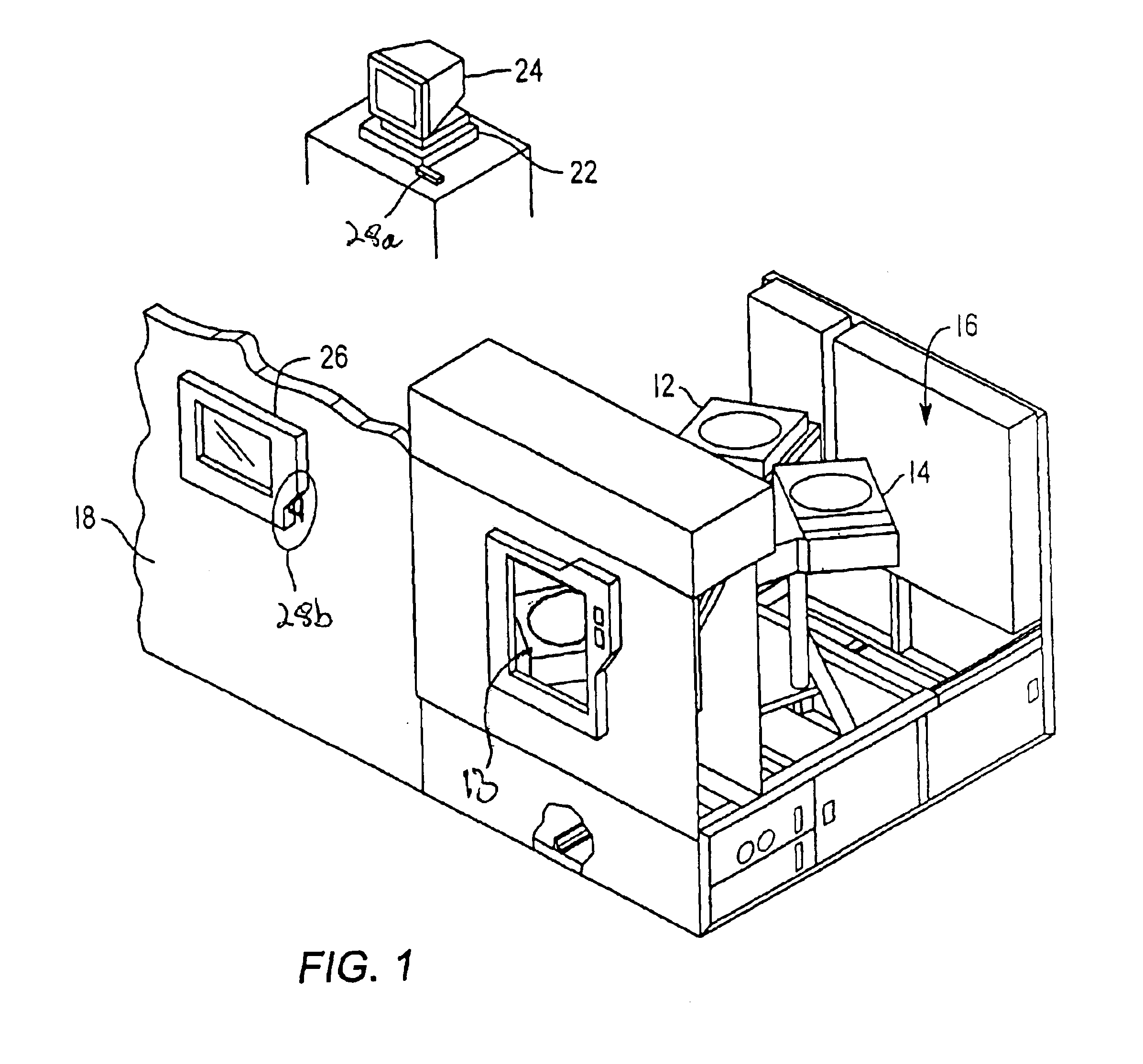
Referring to FIG. 1, an exemplary wafer processing system includes one or more processing chambers 12, 13 and 14 disposed in a common work area 16 surrounded by a wall 18. Processing chambers 12 and 14 are in data communication with a controller 22 that is connected to one or more monitors, shown as 24 and 26. Monitors 24 and 26 typically display common information concerning the process associated with the processing chambers 12 and 14. Monitor 26 is mounted to the wall 18, with monitor 24 being disposed in the work area 16. Operational control of processing chambers 12 and 14 may be achieved with use of a light pen, associated with one of monitors 24 and 26, to communicate with controller 22. For example, a light pen 28a is associated with monitor 24 and facilitates communication with the controller 22 through monitor 24. A light pen 28b facilitates communication with controller 22 through monitor 26.

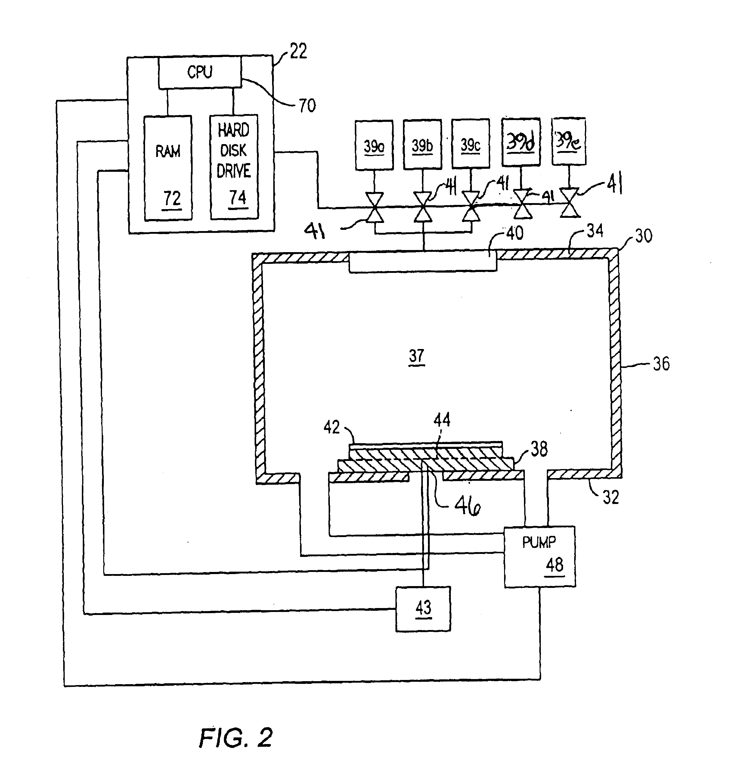
Referring both the to FIGS. 1 and 2, each of processing chambers 12 and 14 includ...


PUM

PropertyMeasurementUnit
Timeaaaaaaaaaa
Timeaaaaaaaaaa
Timeaaaaaaaaaa

Abstract

A system and method to form a stacked barrier layer for copper contacts formed on a substrate. The substrate is serially exposed to first and second reactive gases to form an adhesion layer. Then, the adhesion layer is serially exposed to third and fourth reactive gases to form a barrier layer adjacent to the adhesion layer. This is followed by deposition of a copper layer adjacent to the barrier layer.

Description

BACKGROUND OF THE INVENTIONThis invention relates to the processing of semiconductor substrates. More particularly, this invention relates to improvements in the process of forming contacts.Formation of contacts in multi-level integrated circuits poses many challenges to the semiconductor industry as the drive to increase circuit density continues, due to the reduction in size of the circuit features. Contacts are formed by depositing conductive interconnect material in an opening on the surface of insulating material disposed between two spaced-apart conductive layers. The aspect ratio of such an opening inhibits deposition of conductive interconnect material that demonstrates satisfactory step coverage and gap-fill, employing traditional interconnect material such as aluminum. In addition, diffusion between the aluminum and the surrounding insulating material often occurs, which adversely effects operation of the resulting electrical circuits.Barrier materials have been introduced...

Claims


Application Information

Patent Timeline
IPC IPC(8): H01L21/285H01L21/02H01L21/70H01L21/768H01L21/28C23C16/30H01L21/3205H01L23/52
CPCH01L21/76846H01L21/28562H01L21/768
Inventor MAK, ALFRED W.CHANG, MEIBYUN, JEONG SOOCHUNG, HUASINHA, ASHOKKORI, MORIS
Owner APPLIED MATERIALS INC
Why Eureka
Try Eureka