Wafer processing apparatus and wafer processing method using the same

a technology of wafer processing and processing apparatus, which is applied in the direction of vacuum evaporation coating, transportation and packaging, coatings, etc., can solve the problems of affecting the performance and yield of the resulting semiconductor device, vacuum breakage inevitably occurring in the contact hole, and the conventional integrated cluster tool type wafer processing apparatus does not have all the facilities required, so as to achieve enhanced throughput and reduce contamination of the wafer

Inactive Publication Date: 2005-02-01
SAMSUNG ELECTRONICS CO LTD
View PDF11 Cites 16 Cited by
  • Summary
  • Abstract
  • Description
  • Claims
  • Application Information

AI Technical Summary

Benefits of technology

According to certain embodiments of the invention, exposure to the atmosphere during processing and during the formation of metal wiring layers is eliminated. Therefore, contamination of the wafer may be reduced and throughput may be enhanced.

Problems solved by technology

However, a conventional integrated cluster tool type wafer processing apparatus typically does not have every facility required for performing all the processes for filling a contact hole or a via hole on a wafer.
Accordingly, a vacuum break inevitably occurs during the contact hole or via hole filling processes.
If a wafer is exposed to the atmosphere during the processes for filling a contact hole or a via hole, the exposed surface of the wafer may be contaminated by air, water vapor, or particles in the air, which may adversely affect the performance and yield of the resulting semiconductor device.

Method used


Image

  • Wafer processing apparatus and wafer processing method using the same
  • Wafer processing apparatus and wafer processing method using the same
  • Wafer processing apparatus and wafer processing method using the same

Examples


Embodiment Construction

The present invention now will be described more fully hereinafter with reference to the accompanying drawings, in which various embodiments of the invention are shown. This invention may, however, be embodied in many different forms and should not be construed as limited to the embodiments set forth herein. Rather, these embodiments are provided so that this disclosure will be thorough and complete, and will fully convey the scope of the invention to those skilled in the art. In the drawings, the relative sizes of elements may be exaggerated for clarity. It will be understood that when an element is referred to as being “connected” or “connectable to” another element, it can be directly connected to the other element or intervening elements may also be present.

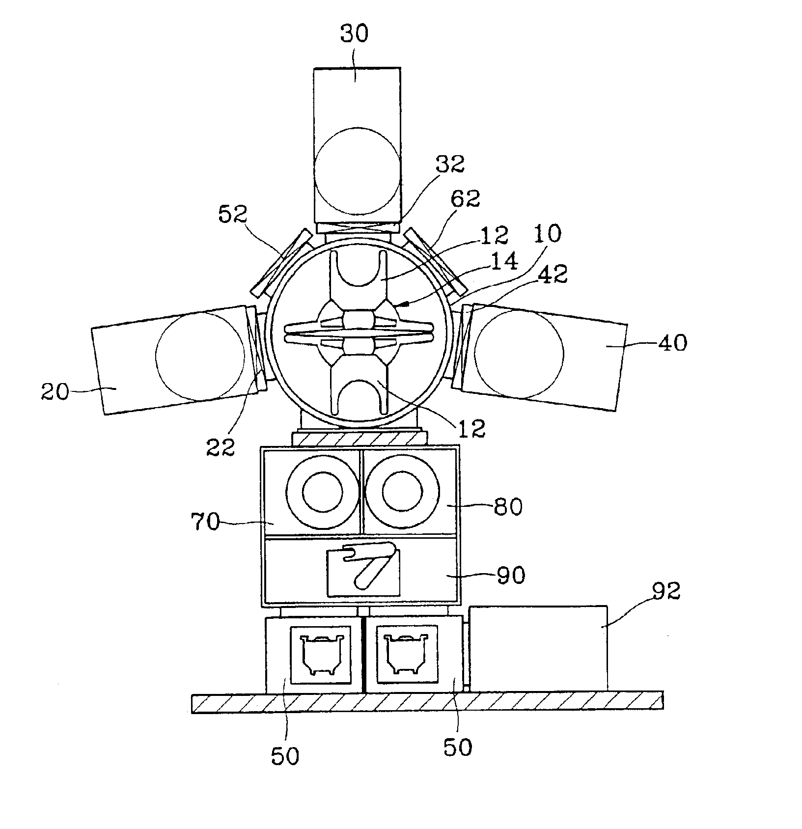
FIG. 1 is a schematic diagram illustrating an integrated in situ cluster tool type wafer processing apparatus according to embodiments of the present invention. Referring to FIG. 1, a wafer processing apparatus according to a...


PUM

PropertyMeasurementUnit
temperatureaaaaaaaaaa
pressureaaaaaaaaaa

Abstract

An integrated in situ cluster type wafer processing apparatus which can be used for forming metal wiring layers having a multi-layered structure and a wafer processing method using the same are provided. The wafer processing apparatus includes a transfer chamber which can be exhausted and has a plurality of gate valves, a plurality of vacuum processing chambers each of which can be connected to the transfer chamber via one of the gate valves, and a load lock chamber which can be exhausted and is connectable to a first gas feed line for feeding an oxygen-based gas into the load lock chamber. In a wafer processing method, a predetermined layer is formed on a wafer in one of the vacuum processing chambers. The predetermined layer on the wafer is oxidized in the load lock chamber or an oxygen atmosphere chamber.

Description

BACKGROUND OF THE INVENTION1. Field of the InventionThe present invention relates to a wafer processing apparatus and a wafer processing method using the same, and more particularly, to a wafer processing apparatus which can be used to form metal wiring layers having a multi-layered structure and a wafer processing method using the same.2. Description of the Related ArtAs the integration density of semiconductor devices increases, it is necessary to introduce metal wiring layers having a multi-layered structure into circuits. Because metal wiring layers transmit electrical signals, it is advantageous to use an economical material for the metal wiring layers which has low electrical resistance and high reliability. To meet these demands, aluminum is widely used for the material of the metal wiring layers. It is also advantageous to electrically connect such aluminum wiring layers in a way that is reliable, economical, and has low electrical resistance. Metal wiring layers are typical...

Claims


Application Information

Patent Timeline
Patent Type & Authority Patents(United States)
IPC IPC(8): H01L21/02H01L21/302H01L21/461C23C14/56C23C16/44H01L21/00H01L21/285H01L21/677H01L21/768
CPCH01L21/2855H01L21/28556H01L21/67017H01L21/67167H01L21/76882H01L21/76888H01L21/67201Y10S438/974H01L21/67739H01L21/02
Inventor LEE, JONG-MYEONGKIM, BYUNG-HEELEE, MYOUNG BUMYUN, JU-YOUNGCHOI, GIL-HEYUN
Owner SAMSUNG ELECTRONICS CO LTD
Why Eureka
Try Eureka