Pulsed processing semiconductor heating methods using combinations of heating sources

Inactive Publication Date: 2005-02-01
MATTSON TECHNOLOGY +1
View PDF20 Cites 137 Cited by
  • Summary
  • Abstract
  • Description
  • Claims
  • Application Information

AI Technical Summary

Benefits of technology

In yet another embodiment, a semiconductor substrate is heated with pulsed energy, and the parameters for the pulse are first determined by estimating the absorptivity of the substrate after a first test pulse (or pre-pulse) of energy is applied. In this method, the substrate is heated to a first temperature below the desired treating or annealing temperature. Then, a first pulse (test pulse or pre-pulse) of energy is applied to heat the substrate to a second temperature greater than the first temperature. Preferably, this second temperature is also below the desired treating temperature, although it is possible to execute the calibration from data obtained after a first treating pulse of energy rather than from a lesser test pulse. During the test pulse, pulse energy data is collected by one or more optical sensors; alternatively or in combination, substrate radiation can also be sensed by one or more pyrometers. The substrate absorptivity is estimated from the sensed data in one of several ways. In one method, one optical sensor detects pulse energy reflected from the substrate, and a second sensor detects pulse energy transmitted through the substrate. The substrate absorptivity is estimated from these two measurements. In a second method, a pyrometer senses the emitted radiation from the front surface of the substrate, providing a means of tr

Problems solved by technology

This creep up in substrate temperature often leads to undesired dopant diffusion, and could cause subsequent applied pulses of equi

Method used


Image

  • Pulsed processing semiconductor heating methods using combinations of heating sources
  • Pulsed processing semiconductor heating methods using combinations of heating sources
  • Pulsed processing semiconductor heating methods using combinations of heating sources

Examples


Embodiment Construction

Apparatus

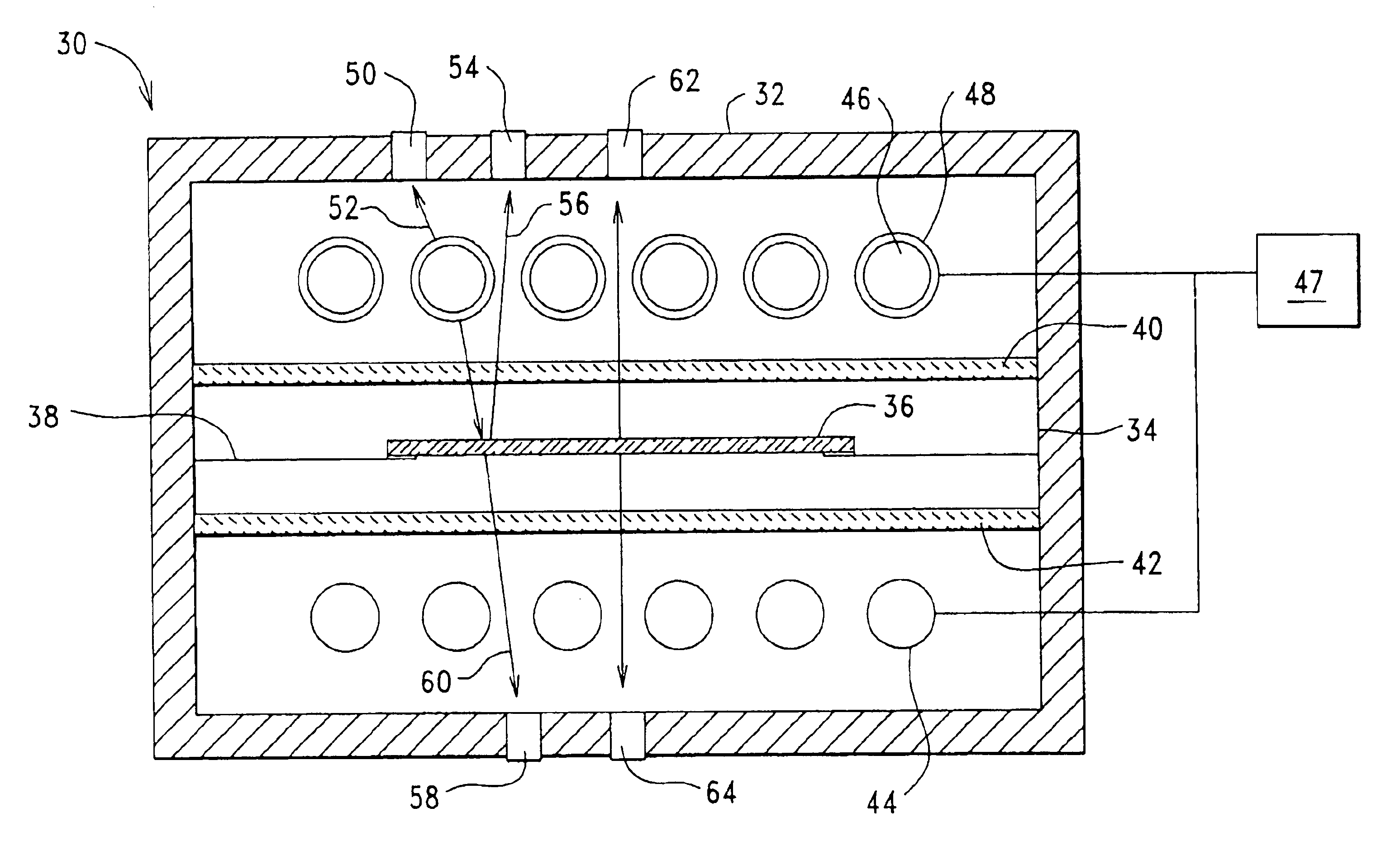
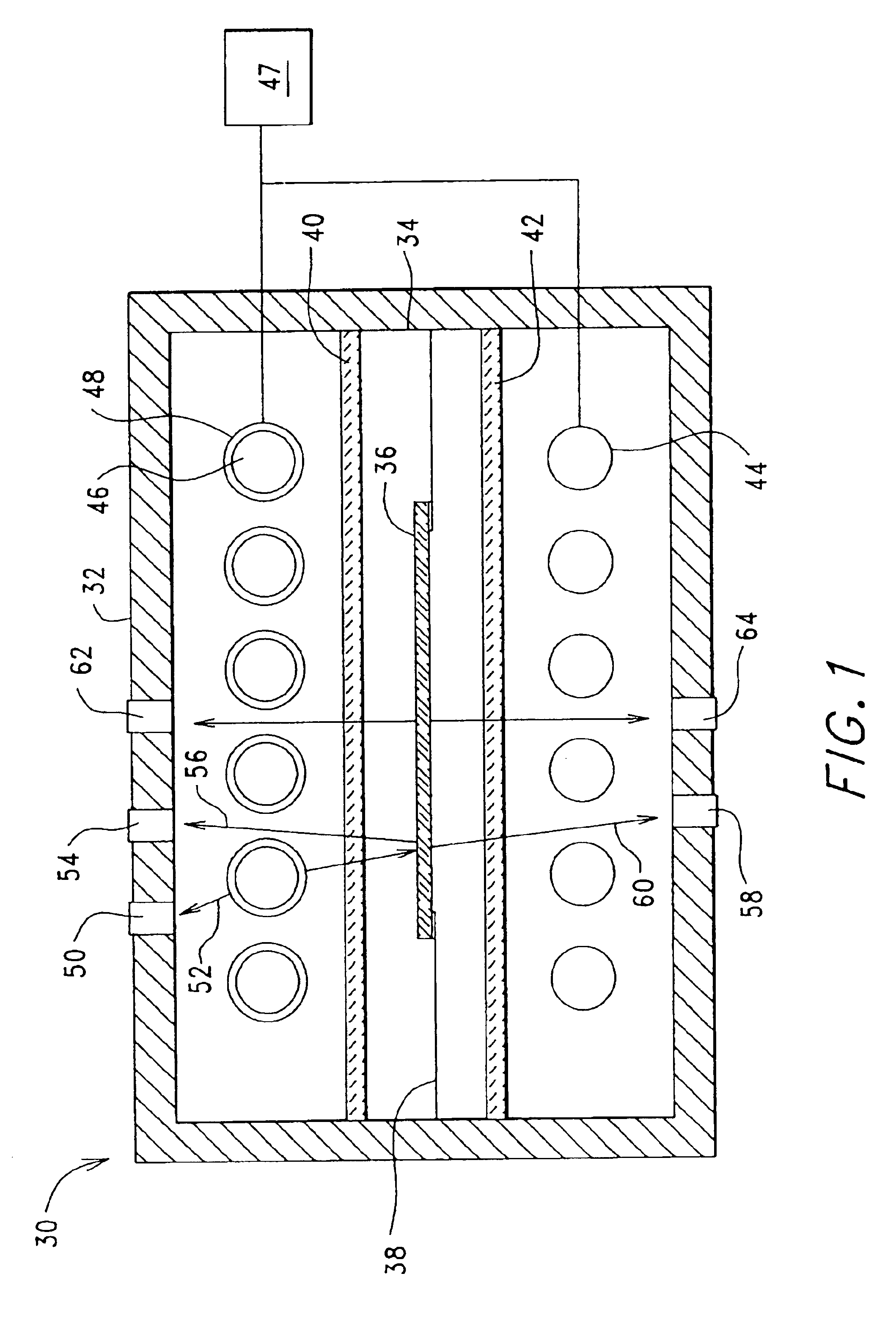
Referring first to FIG. 1, a pulsed processing system 30 includes a housing 32 defining a processing chamber 34 inside which is disposed a substrate 36, such as a semiconductor wafer, held upon a support 38. Quartz windows 40, 42 isolate the substrate 36 and support 38 from heating sources 44, 46 disposed within the housing 32, and are located both above and below the substrate 36. Heat sources 44 and 46 are controlled by a computer / control arrangement 47 which is configured for selectively applying an electrical power level to each of background heating sources 44 and pulsed heating sources 46 to accomplish precise control of both sources. It is noted that control arrangement 47 is readily adaptable for controlling a multimode source in view of this overall disclosure, so as to deliver a heating profile from a single source which combines background heating behavior as well as pulse delivery. Quartz windows 40, 42 may also be water-cooled by providing one or more channels ...


PUM

PropertyMeasurementUnit
Temperatureaaaaaaaaaa

Abstract

Pulsed processing methods and systems for heating objects such as semiconductor substrates feature process control for multi-pulse processing of a single substrate, or single or multi-pulse processing of different substrates having different physical properties. Heat is applied a controllable way to the object during a background heating mode, thereby selectively heating the object to at least generally produce a temperature rise throughout the object during background heating. A first surface of the object is heated in a pulsed heating mode by subjecting it to at least a first pulse of energy. Background heating is controlled in timed relation to the first pulse. A first temperature response of the object to the first energy pulse may be sensed and used to establish at least a second set of pulse parameters for at least a second energy pulse to at least partially produce a target condition.

Description

FIELD OF THE INVENTIONThe present invention relates to methods and systems for heat-treating semiconductor wafers with short, high-intensity pulses, in combination with background heating sources, such as, but not limited to, tungsten-halogen lamps or arc lamps.BACKGROUND OF THE INVENTIONTo make electrical devices, such as microprocessors and other computer chips, a semiconductor wafer such as a silicon wafer, is subjected to an ion implantation process that introduces impurity atoms or dopants into a surface region of a device side of the wafer. The ion implantation process damages the crystal lattice structure of the surface region of the wafer, leaving the implanted dopant atoms in interstitial sites where they are electrically inactive. In order to move the dopant atoms into substitutional sites in the lattice to render them electrically active, and to repair the damage to the crystal lattice structure that occurs during ion implantation, the surface region of the device side of...

Claims


Application Information

Patent Timeline
IPC IPC(8): C30B31/00C30B31/12H01L21/00H05B3/00F27D11/02H01L21/26H01L21/268H05B1/02H05B3/68
CPCC30B31/12H01L21/67248H01L21/67115Y10S438/928H01L21/02H01L21/324
Inventor TIMANS, PAUL J.ACHARYA, NARASIMHA
Owner MATTSON TECHNOLOGY
Why Eureka
Try Eureka