System and method for using film deposition techniques to provide an antenna within an integrated circuit package

a technology of integrated circuit and film deposition technique, applied in the field of antennas, can solve the problems of insufficient area of the substrate on which an antenna is placed, insufficient heat generation of the integrated circuit, and difficulty in reducing so as to reduce the likelihood of rf interference

Inactive Publication Date: 2005-02-01
BELL SEMICON LLC
View PDF14 Cites 42 Cited by
  • Summary
  • Abstract
  • Description
  • Claims
  • Application Information

AI Technical Summary

Benefits of technology

It is an object of the present invention to reduce the likelihood of RF interference with the operation of the IC housed in the package that may be caused by electromagnetic radiation emitted or received by an antenna mounted within the package or adjacent its exterior.

Problems solved by technology

Such alignment may be problematic.
Furthermore, the area of a substrate on which an antenna is placed may be insufficient to provide an antenna of the best physical parameters and geometry.
Also, the vertical stacking of substrates may make the dissipation of heat generated by the integrated circuit difficult.

Method used


Image

  • System and method for using film deposition techniques to provide an antenna within an integrated circuit package
  • System and method for using film deposition techniques to provide an antenna within an integrated circuit package
  • System and method for using film deposition techniques to provide an antenna within an integrated circuit package

Examples


Embodiment Construction

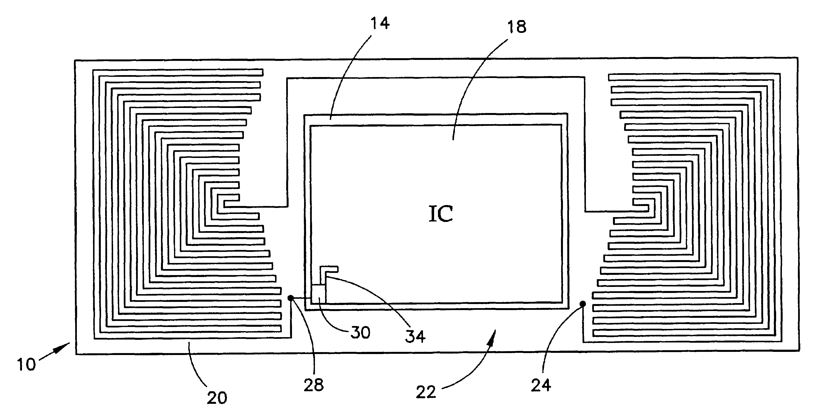
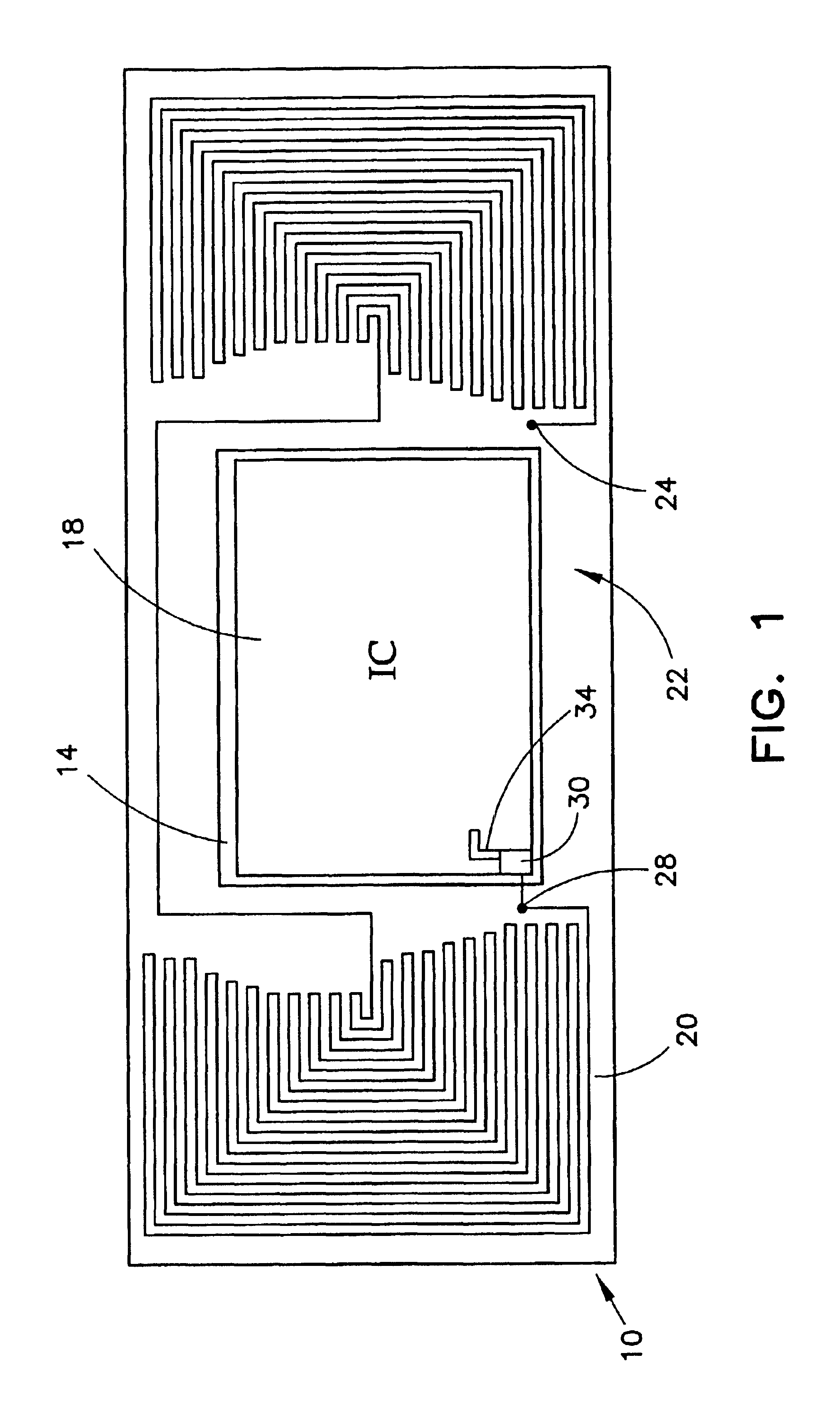
An integrated circuit package 10 of the present invention is shown in FIG. 1 and comprises a cavity 14 for housing an integrated circuit (IC) 18 and an antenna 20 in the interior region 22 of package 10 that lies substantially outside the cavity. Antenna 20 has a terminating end 24 and a coupling end 28. Coupling end 28 may be wire bonded to component pad 30 on IC 18. As shown in FIG. 1, a conductive trace 34 leads from component pad 30 to a component (not shown) of IC 18. The lid that hermetically seals package 10 has been removed to expose the arrangement of antenna 20 with respect to cavity 14.

Antenna 20 may be placed in interior region 22 of IC package 10 by using a damascene process to form trenches in the floor of IC package. Alternatively, the trenches or depressions may be formed with a write process using an electronic beam or a draw process using a laser. Metal is then deposited in the trenches and excess metal may be removed by chemical-mechanical polishing (CMP). The dep...


PUM


Abstract

An integrated circuit package comprises a cavity for housing an integrated circuit (IC) and an antenna provided as part of the package that is located substantially outside the cavity. The antenna may be located on the floor of the IC package that lies in the region outside of the IC cavity. Alternatively, the antenna may be located on the upper or lower surface of the lid sealing the IC package. The antenna may be placed in the floor or on a surface of the IC lid by forming depressions in the floor or lid surface and depositing conductive material in the depressions. The conductive material deposition may be by sputtering, evaporation, or other known physical or chemical deposition method. Antennas formed in the upper surface of an IC lid may be coupled to a pin of the IC package so that the antenna may be electrically coupled to a transceiver component on the IC within the package. Antennas formed in the lower surface of an IC lid or the floor of the IC package may be coupled by a conductive pin to a component pad of the IC within the package. To reduce electromagnetic noise that may be induced by the radio frequency signals emitted or received by an antenna, a grounding plane may be provided as part of the IC package. The grounding plane may be coupled to an electrical ground reference point through an IC package pin or the IC within the package.

Description

FIELD OF THE INVENTIONThis invention relates generally to antennas used with integrated circuits and, more particularly, to antennas coupled to integrated circuits within an integrated circuit package.BACKGROUND OF THE INVENTIONWireless communication devices are becoming increasingly ubiquitous as more peripheral devices are interfaced with voice communication devices and personal digital assistants (PDAs). The demand for wireless communication with peripheral devices has led to the development of the Bluetooth and IEEE 801.11 communication standards. As these communication standards are accepted and incorporated within the integrated circuits used to implement computer peripherals, the need for antennas that radiate and receive communications at radio frequencies (RF), especially those in the 2.4 to 5 GHz range, will increase.One way to meet this need is to provide antennas as additional components in the computer peripherals and other wireless communication devices. Antennas provi...

Claims


Application Information

Patent Timeline
Patent Type & Authority Patents(United States)
IPC IPC(8): H01L23/02H01L23/58H01L23/552H01L23/66H01Q1/22H01Q9/30H01Q23/00
CPCH01L23/552H01L23/66H01L24/19H01Q1/2283H01Q9/30H01Q23/00H01Q1/22H01L2223/6677H01L2924/16152H01L2924/12042H01L2924/14H01L2924/00
Inventor BERMAN, MICHAEL J.BARBER, RENNIE G.
Owner BELL SEMICON LLC
Why Eureka
Try Eureka