Inspection method and apparatus for projection optical systems
a projection optical system and optical system technology, applied in the direction of microlithography exposure apparatus, instruments, measurement devices, etc., can solve the problems of insufficient magnification and image distortion, measurement of overlap error or registration error, and insufficient alone, etc., to achieve accurate measurement of image formation characteristic
- Summary
- Abstract
- Description
- Claims
- Application Information
AI Technical Summary
Benefits of technology
Problems solved by technology
Method used
Image
Examples
first embodiment
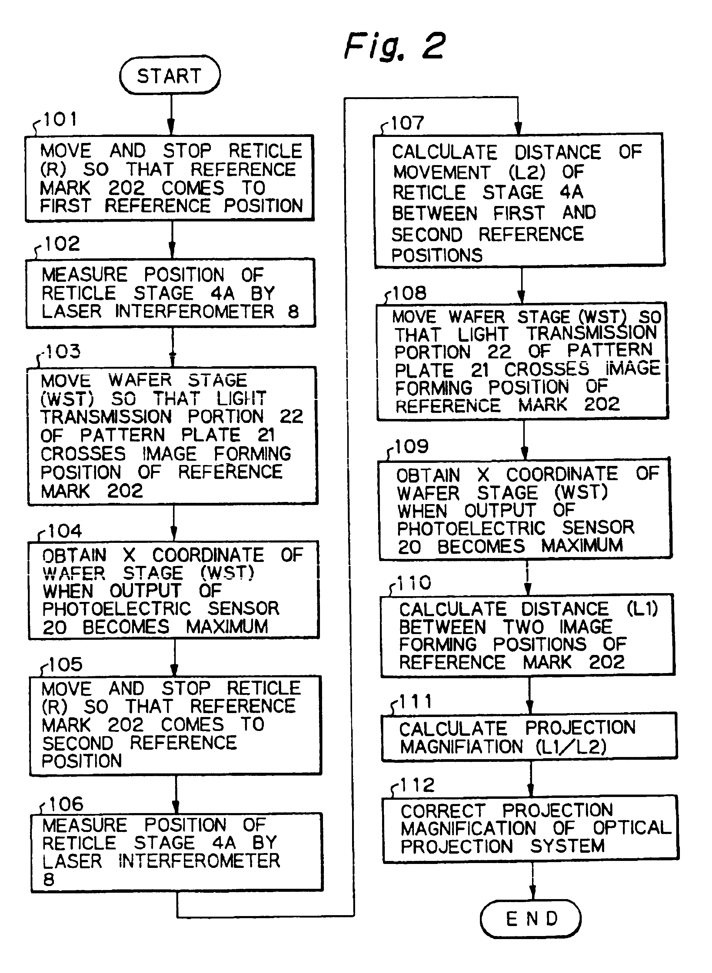
an inspection method for a projection optical system according to the present invention and a projection exposure apparatus for carrying out the inspection method will hereinafter be described in reference to FIG. 2 and FIGS. 4(a) to 4(d). The embodiment of the present invention is applied to a step-and-scan projection exposure apparatus where patterns on a reticle (photomask) are serially transferred on shot areas of a semiconductor wafer (photosensitive substrate) while scanning the reticle and the wafer in synchronization with each other.
FIG. 3 schematically illustrates the projection exposure apparatus of this embodiment. In the figure, reference character IL denotes illumination light (e.g., bright-line such as a g-line or an i-line in a ultraviolet spectral region) emitted from a light source 1 comprising an extra-high pressure mercury vapor lamp. The illumination light IL passes through a shutter (not shown) and is converted to luminous flux whose illuminance distribution is ...
second embodiment
Now, the present invention will be described in reference to FIGS. 7(a) and 7(b). While in the first embodiment a space image has been measured, in this embodiment an image is transferred on the photoresist (photosensitive material) covering the surface of the wafer W and the transferred image is measured. The aforementioned measurement of the space image can be used as a convenient measuring method, but since an actual pattern is formed in the photoresist, finally the system needs to be inspected with the resist image for manufacturing a final product. The reason is that there are some cases where the space image does not match completely with the measured value because of the characteristic of the photoresist and the aberration of the projection optical system PL.
Briefly explained, the photoresist is in two states; an exposed state and an unexposed state, but the space image is a continuous value. Therefore, it is considered that the influence of the aberration of the projection o...
third embodiment
Now, the present invention will be described in reference to FIG. 8 and FIGS. 9(a) through 9(c). In this embodiment, a plurality of reference marks are formed on the reticle R, and using the laser interferometer of the exposure apparatus, the drawing error of the reticle R is obtained while actually measuring the error.
FIGS. 9(a) to 9(c) are diagrams used to explain the operation of the reticle R. FIG. 9(a) shows the state where the position of a reference mark 506 is being measured, FIG. 9(b) shows the state where the position of a reference mark 507 is being measured, and FIG. 9(c) shows the state where magnification is being measured actually. As shown in FIGS. 9(a) to 9(c), this embodiment is identical in construction with the first embodiment, except that the reticle R is provided with two reference marks 506 and 507, the pattern plate 30 used in the modification of the first embodiment is used as a pattern plate of the wafer stage WST, and two photoelectric sensors 20A and 20B...
PUM
| Property | Measurement | Unit |
|---|---|---|
| reflection | aaaaa | aaaaa |
| area | aaaaa | aaaaa |
| time | aaaaa | aaaaa |
Abstract
Description
Claims
Application Information


