Semiconductor production system

a production system and semiconductor technology, applied in the field of semiconductor production systems, can solve the problems of affecting the overall performance of the system, inevitably increasing traffic, and degrading the performance of the network, and achieve the effects of improving system throughput, high speed, and large volum

Inactive Publication Date: 2005-02-01
HITACHI LTD
View PDF21 Cites 294 Cited by
  • Summary
  • Abstract
  • Description
  • Claims
  • Application Information

AI Technical Summary

Benefits of technology

As described above, with this invention because the semiconductor manufacturing apparatus or storage devices are linked together via the storage area network, a large volume of image data or design data can be transferred at high speed, improving the system throughput.

Problems solved by technology

In the conventional technologies described above, because two kinds of data, namely a large volume of CAD data representing design information on semiconductors and semiconductor masks and message data representing control commands for controlling and linking a variety of devices are transferred on the same network without considering the kind of data flowing through the network, traffic inevitably increases, degrading the performance of the network, which in turn adversely affects the overall performance of the system.
That is, the conventional networks have a problem that the throughput of the networks changes according to the frequency of issuing the control command, the frequency of generating a response to the command and the transmission / reception of a large volume of data such as image data, thus degrading the overall performance of the apparatus.
This adversely affects the transmission and reception of message data.
In this case, however, because the processing stations copy data between the segments, the processing stations themselves become a bottleneck of the overall performance of the system.
For example, if the inspection apparatus and manufacturing apparatus are connected together via network, data must be copied via network in order to transfer data between these apparatus, thus crowding the network and lowering the throughput of the system as a whole.
Further, it is also necessary to copy data between storage devices connected to individual segments and this makes the consistency management of copied data complicated.

Method used


Image

  • Semiconductor production system
  • Semiconductor production system
  • Semiconductor production system

Examples


Embodiment Construction

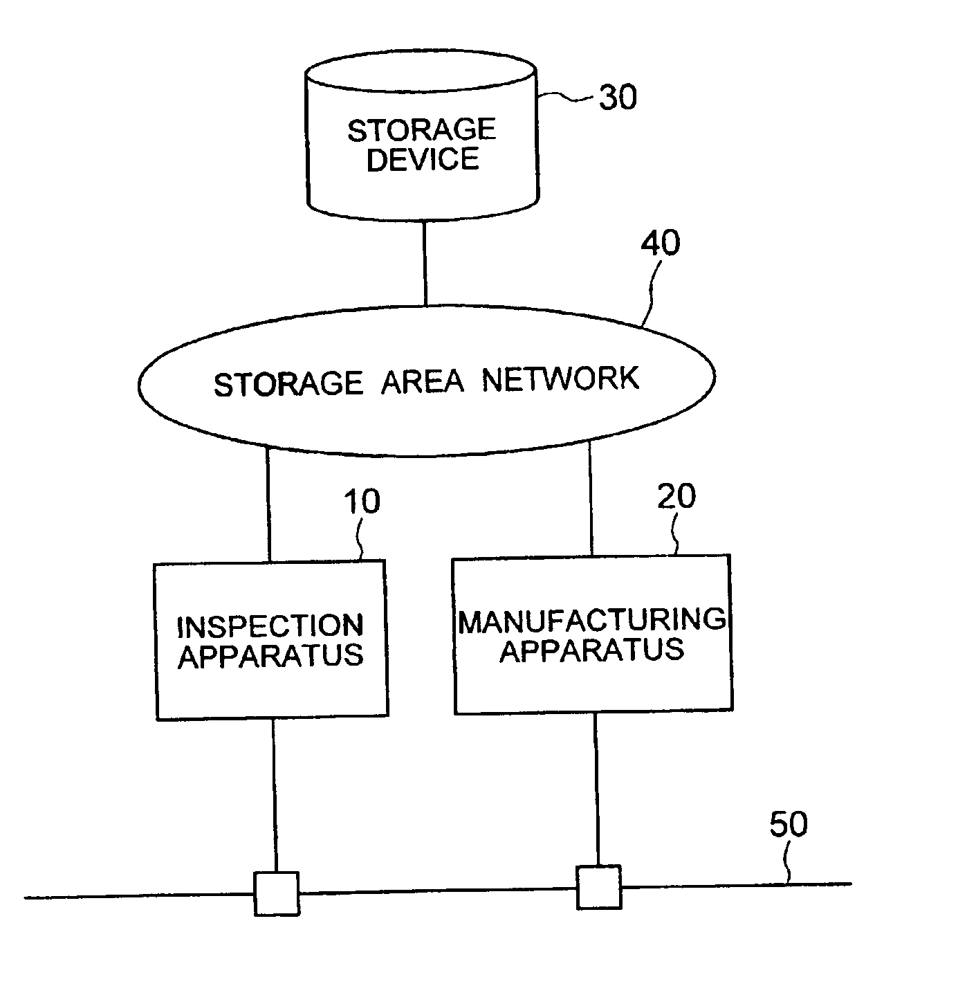
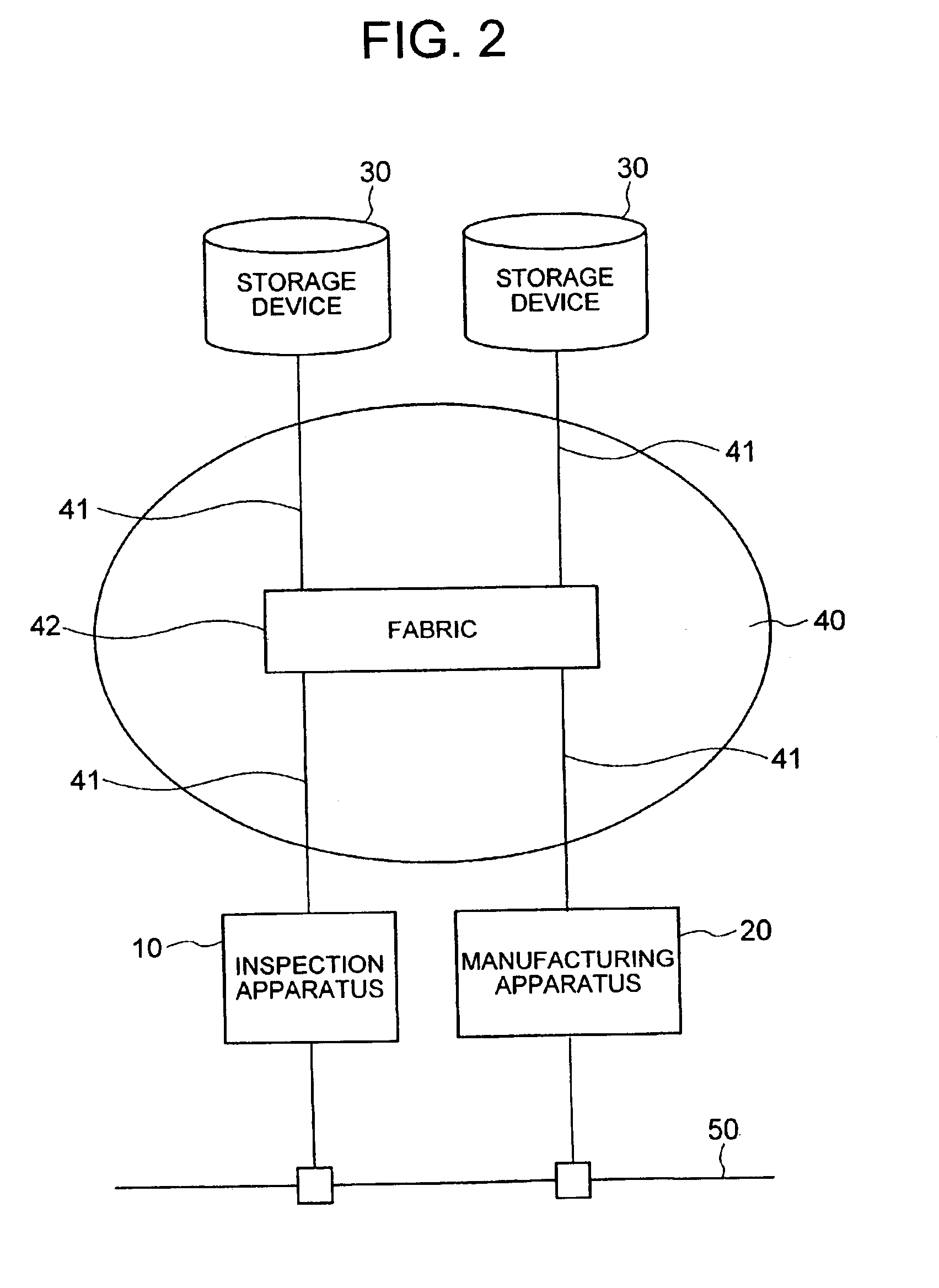
Embodiments of the present invention will be described by referring to FIG. 1 to FIG. 32. FIG. 1 is a block diagram showing a semiconductor production system as one embodiment of-the present invention.

As shown in the figure, a storage area network 40 interconnects a semiconductor inspection apparatus 10, a semiconductor manufacturing apparatus 20 and a storage device 30. The semiconductor inspection apparatus 10 and the semiconductor manufacturing apparatus 20 can also be interconnected via a general network 50. In this embodiment, the provision of the storage area network 40 achieves a large-capacity data communication between the semiconductor inspection apparatus 10 and the semiconductor manufacturing apparatus 20 without affecting the general network 50. Because the storage device 30 is shared by the semiconductor inspection apparatus 10 and the semiconductor manufacturing apparatus 20, data does not have to be copied between the apparatus, thus improving the overall performance...


PUM

PropertyMeasurementUnit
storage areaaaaaaaaaaa
proximity effectaaaaaaaaaa
proximity effect correctionaaaaaaaaaa

Abstract

A semiconductor production system has a semiconductor manufacturing apparatus having an exposure unit, a control unit for controlling the exposure unit and a storage device; a semiconductor inspection apparatus having an observation unit, a control unit for controlling the observation unit and a storage device; and a storage device commonly used by the semiconductor manufacturing apparatus and the semiconductor inspection apparatus. The manufacturing apparatus, the inspection apparatus and the commonly used storage device are interconnected via a storage area network. With the semiconductor manufacturing apparatus and the storage device linked together via the storage area network, a large volume of image data or design data can be communicated at high speed, thus improving the system throughput.

Description

BACKGROUND OF THE INVENTIONThe present invention relates to a semiconductor production system and more particularly to a semiconductor production system linking a semiconductor manufacturing apparatus, an inspection apparatus and a storage device by using a storage area network.A commonly used communication means for interconnecting apparatus is a LAN (local area network) described, for example, in Japanese Patent Unexamined Publication No. 2000-164667. Another system is also known which, as disclosed in Japanese Patent Unexamined Publication No. 9-153441 (corresponding to U.S. Pat. No. 5,867,389), divides a LAN into a plurality of segments and installs a processing station between the divided segments to copy data.The storage area network is an independent network which is constructed of only storages, devices for storing data, by separating the storages from a server. Examples of such storage area networks include those networks based on such links as a fiber channel (one of seria...

Claims


Application Information

Patent Timeline
Patent Type & Authority Patents(United States)
IPC IPC(8): G03F7/20H01L21/00G01R31/26G01R31/28H01L21/02H01L21/027H01L21/66
CPCG03F7/70508G03F7/70991G05B19/418G05B19/41855H04L67/1097H01L21/67225H01L21/67276G05B2219/31326G05B2219/45031G05B2219/31323Y02P90/02H01L21/02
Inventor NAYA, HIDEMITSUTOMIYOSHI, RIKIOMORIYAMA, SHIGEOKIKUCHI, MUTSUMISHIMAMURA, KOTARO
Owner HITACHI LTD
Why Eureka
Try Eureka