Carbon nanotube gate field effect transistor

a carbon nanotube and gate technology, applied in the field of carbon nanotube gate field effect transistor, can solve the problems of limited device size in this prior art and limited gate width of transistor, and achieve the effect of greatly decreasing the gate width

Inactive Publication Date: 2005-02-08
IND TECH RES INST
View PDF3 Cites 59 Cited by
  • Summary
  • Abstract
  • Description
  • Claims
  • Application Information

AI Technical Summary

Problems solved by technology

But the gate width of transistor is still limited by conventional process of sputtering, metal-screen-printing and etching.
So the size of device in this prior art is limited by the process of semiconductor.

Method used


Image

  • Carbon nanotube gate field effect transistor
  • Carbon nanotube gate field effect transistor
  • Carbon nanotube gate field effect transistor

Examples


Embodiment Construction

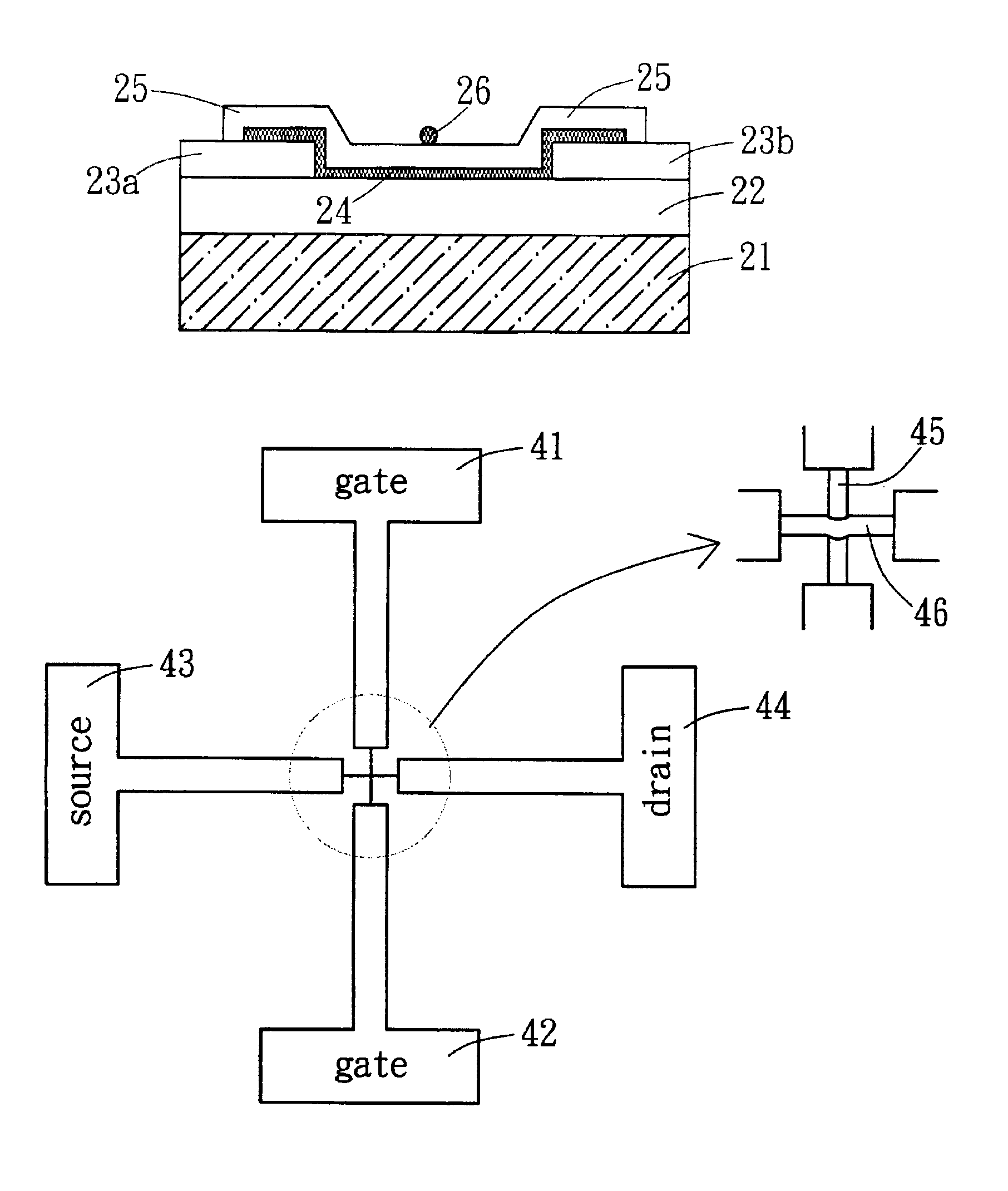
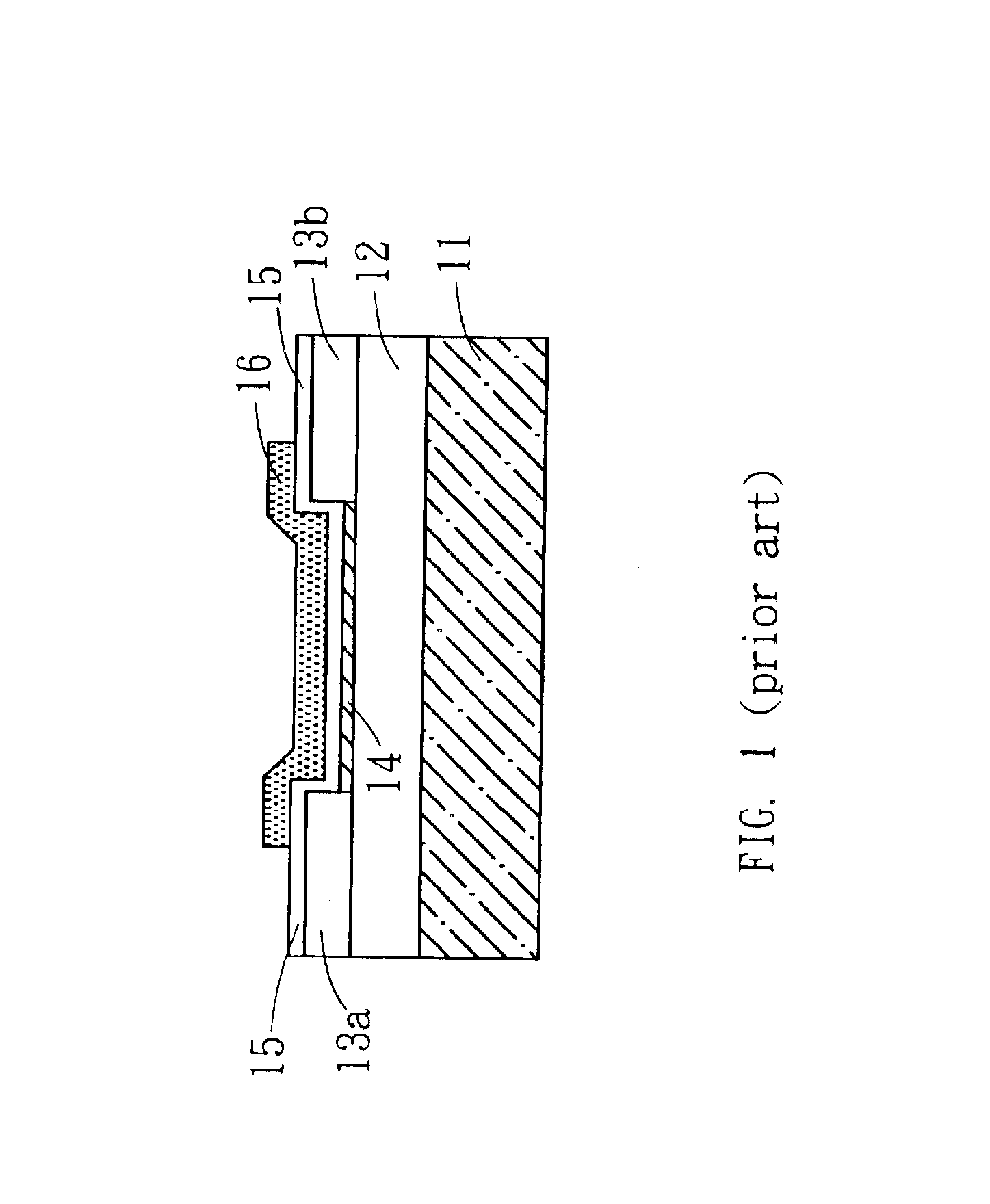
The present invention relates to an apparatus and method of carbon nanotube (CNT) gate field effect transistor (FET), which is used to replace the current metal gate of transistor. That can decrease the gate width greatly to the nano-scale range, and work well in this kind of scale. Also, the carbon nanotube has its own intrinsic characters of metal and semiconductor, so the gate, source and drain of the transistor can be exchanged. Then, it can be defined the device's specificity by outside wiring, and present the same characters with regular transistor.

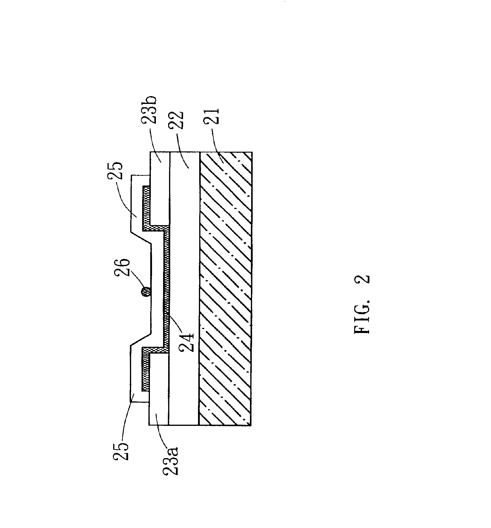
Please refer to FIG. 2, which is a schematic diagram showing the structure of carbon nanotube gate transistor in accordance with one preferred embodiment of the present invention. To begin with, there is a silicon substrate 21 existed on the bottom layer, and there is another isolated layer 22 deposited above, the isolated layer 22 is usually implemented by oxide material. Then, to deposit source 23a and drain 23b of transistor on t...


PUM


Abstract

The present invention generally relates to an apparatus and method of carbon nanotube (CNT) gate field effect transistor (FET), which is used to replace the current metal gate of transistor for decreasing the gate width greatly. The carbon nanotube has its own intrinsic characters of metal and semiconductor, so it can be the channel, connector or next-level gate of transistor. Furthermore, the transistor has the structure of exchangeable source and drain, and can be defined the specificity by outside wiring.

Description

BACKGROUND OF THE INVENTION1. Field of the InventionThe invention relates to an apparatus and manufacturing process of carbon nanotube gate FET, for the carbon nanotube can be the channel, connector or next-level gate of transistor, and the source and drain of transistor can be exchanged and defined the specificity by outside wiring.2. Description of the Prior ArtAs entering the age of nano scale, the device is getting smaller, so fabricating the nano-scale devices using nano-scale matter becomes the trend of progress, eg. the CNT-FET bases on CNT material. But the gate width of transistor is still limited by conventional process of sputtering, metal-screen-printing and etching.Please refer to FIG. 1, which is a schematic diagram showing the structure of carbon nanotube transistor in the prior art. First at all, depositing an oxide layer 12 above a silicon substrate 11, and the oxide layer 12 could be SiO2. Then depositing a metal thin film to be source 13a and drain 13b respectivel...

Claims


Application Information

Patent Timeline
Patent Type & Authority Patents(United States)
IPC IPC(8): H01L21/02H01L21/337H01L29/40H01L21/3205H01L29/43H01L21/4763H01L51/00H01L51/05H01L51/10H01L51/30H03K5/00H03K17/00
CPCB82Y10/00H01L51/0021H01L51/0541H01L51/102H01L51/105H01L51/0048Y10S977/938H01L51/0052H10K71/60H10K85/221H10K85/615H10K10/464H10K10/82H10K10/84
Inventor WEI, JENG-HUACHEN, HSIN-HUILAI, MING-JIUNNWANG, HUNG-HSIANGKAO, MING-JER
Owner IND TECH RES INST
Why Eureka
Try Eureka