Bandgap reference circuit

a reference circuit and bandgap technology, applied in the field of circuits, can solve the problems of inability of the amplifier to supply the network of resistors and diodes, and the inertness of the bandgap reference circuit, and achieve the effects of low power consumption, improved stability, and moderate accuracy

Inactive Publication Date: 2005-02-08
SEMICON COMPONENTS IND LLC
View PDF9 Cites 17 Cited by
  • Summary
  • Abstract
  • Description
  • Claims
  • Application Information

AI Technical Summary

Benefits of technology

One embodiment of the invention relates to a practical, relatively simple bandgap (BG) reference circuit with complementary metal oxide semiconductor (CMOS) transistors or bipolar transistors. The BG reference circuit advantageously provides moderate accuracy and low power consumption in a wide range of temperatures and input voltages. The BG reference circuit provides better stability and a low cost production yield. In one configuration, the BG reference circuit specifications include a maximum + / −6 mV voltage change in a temperature range of −40° C. to +125° C. and between about 2-V to 8-V power supply. This means that the bandgap voltage (BG)=1.240V + / −6 mV.
The bandgap reference circuits and methods described herein may be implemented in several products or applications without any adverse effects. One advantage of the circuits and methods is their relative simplicity. In one embodiment, a two-stage op amp may be used, and no starting loop is necessary. The risk of oscillation is strongly reduced, and the power supply current is reduced as well.

Problems solved by technology

With a low output, the op amp is not able to supply the network of resistors and diodes, and thus the bandgap reference circuit remains inert.

Method used


Image

  • Bandgap reference circuit
  • Bandgap reference circuit
  • Bandgap reference circuit

Examples


Embodiment Construction

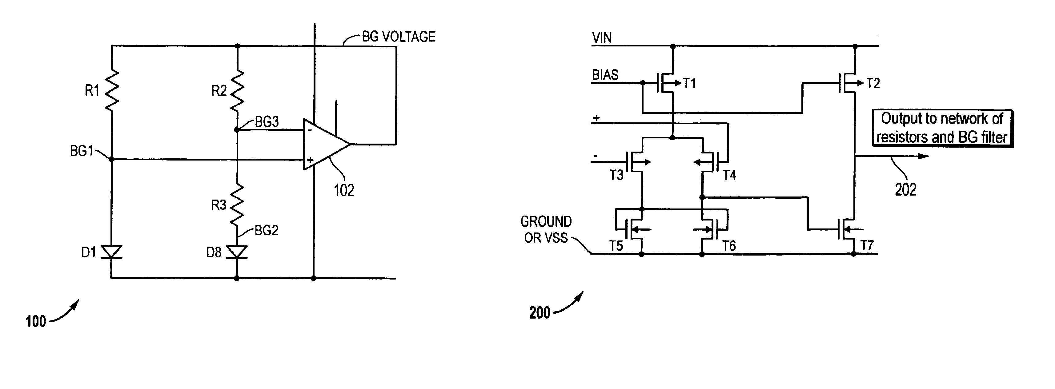
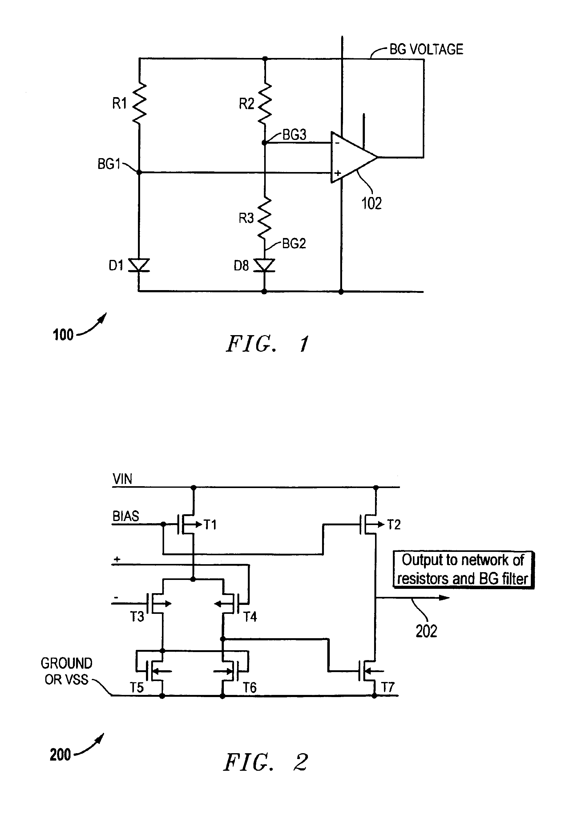
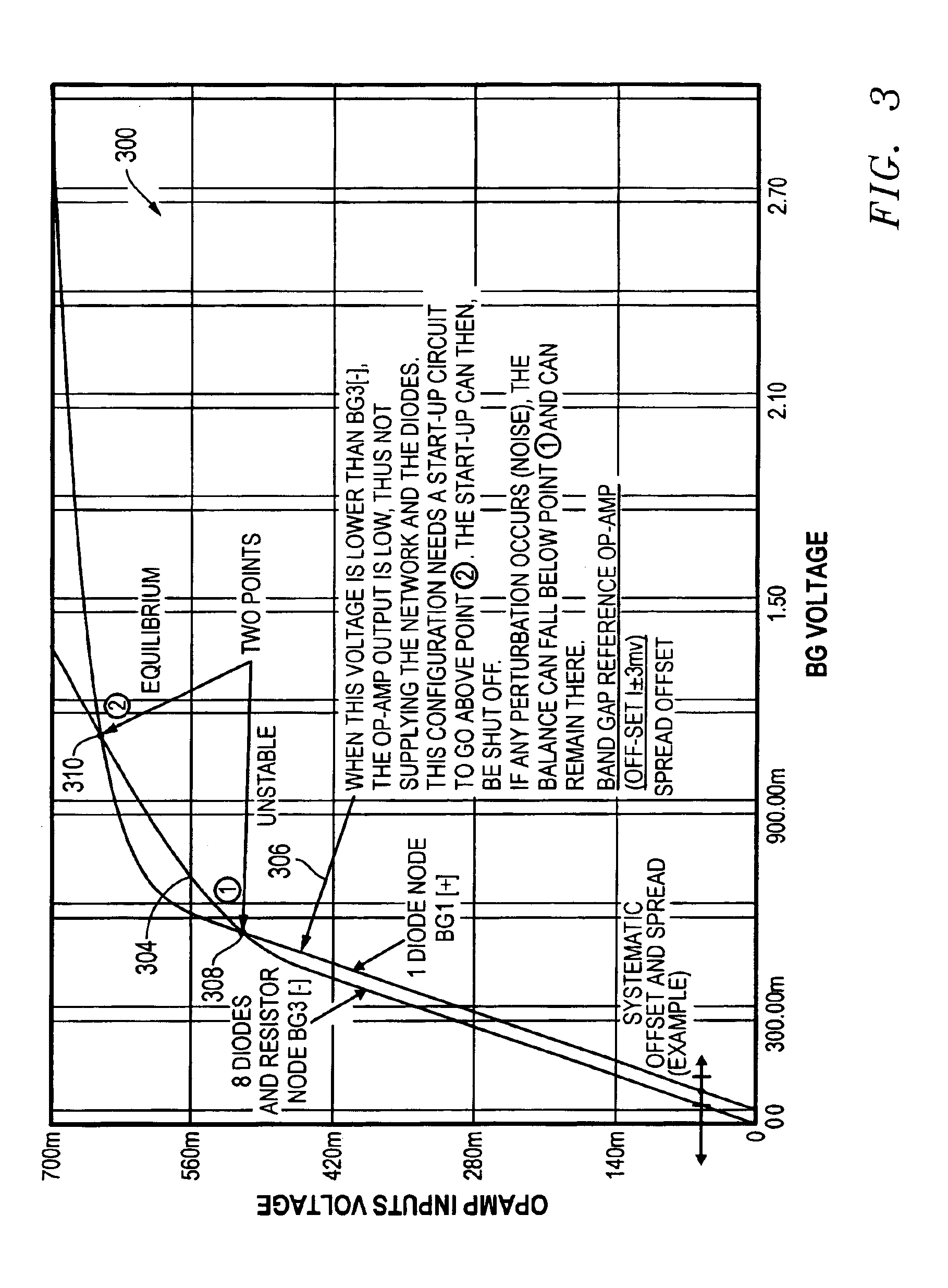
FIG. 1 illustrates one embodiment of a bandgap (BG) reference circuit 100. The circuit 100 comprises a resistor R1, a first bandgap node (or test point) BG1, a first diode D1, another resistor R2, a third bandgap node BG3, another resistor R3, a second bandgap node BG2, a set of diodes D8 in parallel, an amplifier 102, such as an operational amplifier, and a bandgap voltage BG line / node / test point. The circuit 100 may comprise other components in addition to or instead of the components shown in FIG. 1.

In one embodiment, the diodes D1, D8 are identical bipolar diodes. The set of diodes labeled “D8” may comprise eight diodes in parallel. In other embodiments, less than eight or more than eight diodes may be used in the set labeled as “D8.” The difference in voltage between the forward-biased diode D1 (voltage at BG1) and the set of diodes D8 in parallel (voltage at BG2), may be represented as dV:

dV=BG1−BG2

The dV value may increase with a rising temperature, while the BG1 and BG2 valu...


PUM

PropertyMeasurementUnit
bandgap reference voltageaaaaaaaaaa
temperatureaaaaaaaaaa

Abstract

A bandgap reference circuit and method of using the same are provided. The bandgap reference circuit may provide start-up requirements at substantially any voltage and at substantially any temperature. The circuit comprises an op amp (two stages of transistors) and a network of resistors and bipolar diodes. When an artificial offset of about −5 mV is introduced to the op amp, the op amp output will be high as soon as the power supply exceeds the transistors' threshold voltages. The op amp output supplies the resistor and diode network and brings the op amp inputs within desired regulation voltages.

Description

BACKGROUND OF THE INVENTION1. Field of the InventionThe present invention relates to circuits, and in particular to bandgap reference circuits.2. Description of the Related ArtIdeally, a bandgap reference circuit is intended to provide a substantially temperature-invariant reference voltage level to other circuits over a range of temperatures. The bandgap reference circuit is an electrical loop that needs a means of starting the circuit, such as a start-up circuit. Most of the time, the means of starting the bandgap reference circuit can consume current (i.e., drain power) and, in some cases, be a source of oscillation or instability.A “positive offset” is defined as an output of an operational amplifier (op amp) being relatively low when the differential pair inputs of the op amp are connected to substantially the same voltage. Conversely, a “negative offset” causes the op amp output to be at a relatively high level. A “systematic offset” is an offset introduced by a design princip...

Claims


Application Information

Patent Timeline
Patent Type & Authority Patents(United States)
IPC IPC(8): G05F3/08G05F3/30H03K17/22
CPCG05F3/30H03K17/223
Inventor PRINZ, FRANCOIS X.AIOANEI, OVIDIU
Owner SEMICON COMPONENTS IND LLC
Why Eureka
Try Eureka