Silicon-on-insulator channel architecture for automatic test equipment

a silicon-on-insulator and automatic test technology, applied in the direction of resistance/reactance/impedence, measurement devices, instruments, etc., can solve the problems of increasing the pin count of modern semiconductor devices, expensive filtering systems, and large and/or higher channel cards. achieve the effect of sacrificing performan

Active Publication Date: 2005-02-08
TERADYNE
View PDF2 Cites 11 Cited by
  • Summary
  • Abstract
  • Description
  • Claims
  • Application Information

AI Technical Summary

Benefits of technology

The channel architecture described herein enables multi-voltage levels on the same integrated circuit without sacrificing performance. This provides the capability of minimizing the number and size of channel cards employed in automatic test equipment.

Problems solved by technology

While this has worked well in many instances, modern semiconductor devices are increasing in pin count, requiring additional channel resources from the tester to adequately test the devices.
Having separate integrated circuits for channel resources running on different voltage levels undesirably leads to larger and / or higher numbers of channel cards.
Semiconductors are often tested in “clean rooms.” A clean room has expensive filtering systems to keep dust and other impurities from corrupting the semiconductor devices, particularly before they are encased in a package.
Each square foot of clean room space is very expensive to build and operate.
Cost is also an important issue for semiconductor device manufacturers.
The cost of the silicon occupied by the circuitry inside an integrated circuit represents a small fraction of the overall cost of the device.
Packaging the silicon, building a circuit board to hold the device, building a frame to hold the printed circuit boards all add substantial costs to the finished product.
All of these costs increase with the number of integrated circuit chips.
This unevenness typically occurs because of the common transistor bulk connections at Bp and Bn (in phantom).
For applications needing high performance switching speeds, the conventional stacking technique is often unacceptable.

Method used


Image

  • Silicon-on-insulator channel architecture for automatic test equipment
  • Silicon-on-insulator channel architecture for automatic test equipment
  • Silicon-on-insulator channel architecture for automatic test equipment

Examples


Embodiment Construction

The channel architecture described herein provides a way to combine relatively high voltage and low voltage circuits on the same integrated circuit chip without incurring undesirable performance degradation. This is accomplished by forming the various circuits in accordance with silicon-on-insulator process technology.

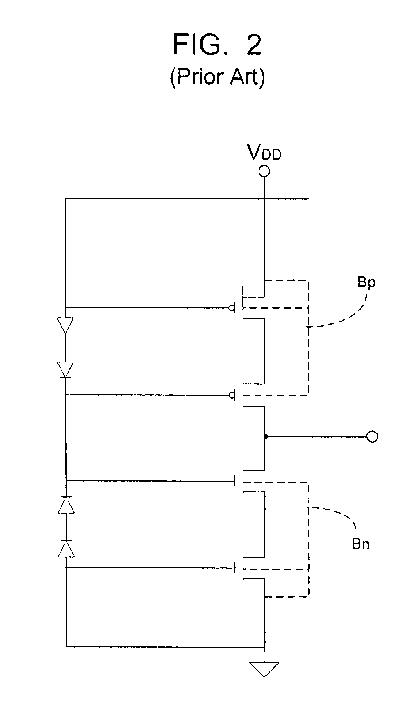
FIG. 3 illustrates a basic stacked CMOS inverter array suitable for use in the channel architecture described herein, and enabled by the use of a silicon-on-insulator (SOI) process. The inverter array includes a pair of p-channel transistors QP1 and QP2 disposed in series between a source voltage VDD and a pair of n-channel transistors QN1 and QN2. The node formed by the connection of the p-channel and n-channel transistors forms the inverter output OUT. An array of diodes D1-D4 coupled to the gates of the p-channel and n-channel transistors and the source voltage VCC provide voltage inputs of differing levels. The n-channel transistors are configured to complement the...


PUM


Abstract

A channel architecture for use in automatic test equipment is disclosed. The channel architecture comprises pattern generation circuitry and timing circuitry responsive to the pattern generation circuitry to generate timing signals. Formatting circuitry coupled to the output of the timing circuitry generates pulse waveforms for application to pin electronics circuitry. The pin electronics circuitry is responsive to the formatting circuitry for interfacing the automatic test equipment to a device-under-test. The pattern generation circuitry, the timing circuitry, the formatting circuitry and the pin electronics circuitry are formed on the same integrated circuit.

Description

FIELDThe invention relates generally to automatic test equipment, and more particularly a channel architecture formed with a silicon-on-insulator process for automatic test equipment applications.BACKGROUNDAutomatic test equipment provides semiconductor device manufacturers the ability to test each and every device fabricated. By testing each device, the manufacturer can sort devices having like speeds, and / or separate failed devices from passing devices. In this manner, the manufacturer is able to confidently put fully functioning devices into the marketplace.FIG. 1 illustrates a typical semiconductor tester, generally designated 10. The tester includes a controller or computer workstation 12 coupled to a testhead 14. The testhead houses large circuit boards, or channel cards 16 that mount the electronics necessary for interfacing with one or more devices-under-test 18 (DUTs). In some instances, the controller may be integrated within the testhead, such that the entire tester compr...

Claims


Application Information

Patent Timeline
Patent Type & Authority Patents(United States)
IPC IPC(8): G01R31/28G01R31/319
CPCG01R31/31924G01R31/31905
Inventor OSTERTAG, EDWARD
Owner TERADYNE
Why Eureka
Try Eureka