HBT and field effect transistor integration

a transistor and field effect technology, applied in the field of device fabrication, can solve the problems of limiting reproducibility and control, bifet performance, etc., and achieve the effect of reducing avoiding the degradation of the fet devi

Active Publication Date: 2011-04-12
MICROLINK DEVICES
View PDF5 Cites 3 Cited by
  • Summary
  • Abstract
  • Description
  • Claims
  • Application Information

AI Technical Summary

Benefits of technology

[0008]The ability to combine the structures of FETs and HBTs onto a single substrate offers a wide variety of structures, operational characteristics, and functions that can be integrated into a compact size, which reduces the total circuit footprint and improves the operational characteristics of the circuit. This has led to the development of transistors that integrate HBTs and FETs in order to take advantage of the strengths of each device type. One potential application for a BiFET device is a Transmitter / Receiver module (T / R module), where a low noise amplifier, a power amplifier, switches, and phase shifters can all be integrated onto a single chip without degrading the operational characteristics of the FET device or the HBT device.
[0009]There are a number of advantages to the methods described herein over the conventional single-growth-cycle, common growth environment methodologies. Aside from those advantages already described, the methodologies of the present invention allow the performance of the FET device to be separately evaluated before formation of the HBT device is performed. Moreover, high performance circuits based on either a FET device or an HBT device can be fabricated using a single wafer. In addition, the design and fabrication of FET and HBT devices can be separately optimized without sacrificing performance.
[0010]Moreover, the integration of a FET and HBT in accordance with the teachings of the present invention offers numerous mixed signal applications which have been difficult to achieve using conventional methodologies. Conventionally, different functionalities are implemented on a circuit board using separate chips. By integrating functions, such as a power amplifiers, switches, bias controls, and low noise amplifiers, on a single chip, the chip count and packaging cost can be reduced.
[0012]According to another embodiment, the FET portion of the BiFET device is substantially free of contamination from impurities introduced during formation of the HBT portion of the BiFET device. The FET may be from the HFET subfamily, for instance, a pHEMT. In addition, the substrate on which the FET is formed may be one of a GaAs or InP substrate.
[0013]According to another embodiment, the temperature is lowered during the forming of the HBT portion of the BiFET device to avoid the degradation of the FET device. The temperature in one embodiment is lowered between 30° C. and 100° C. from a customary temperature used during formation of an HBT device.
[0014]According to another embodiment, a reduced oxide desorption process is applied, where the temperature of the substrate is lowered by about 50-100° C. between the formation of the FET and the formation of the HBT to reduce the degradation of the FET device.

Problems solved by technology

However, the resulting BiFET performance is compromised since the growth of highly doped materials from the HBT device introduces impurities into the subsequent growth of the FET device, which limits the reproducibility and control.

Method used


Image

  • HBT and field effect transistor integration
  • HBT and field effect transistor integration
  • HBT and field effect transistor integration

Examples


Embodiment Construction

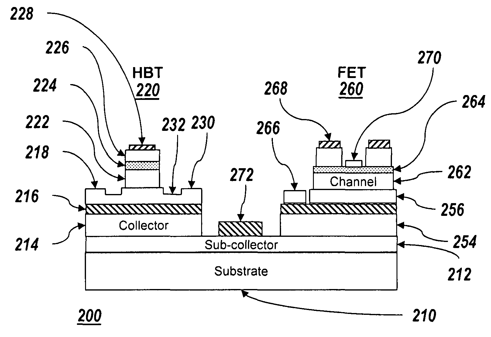
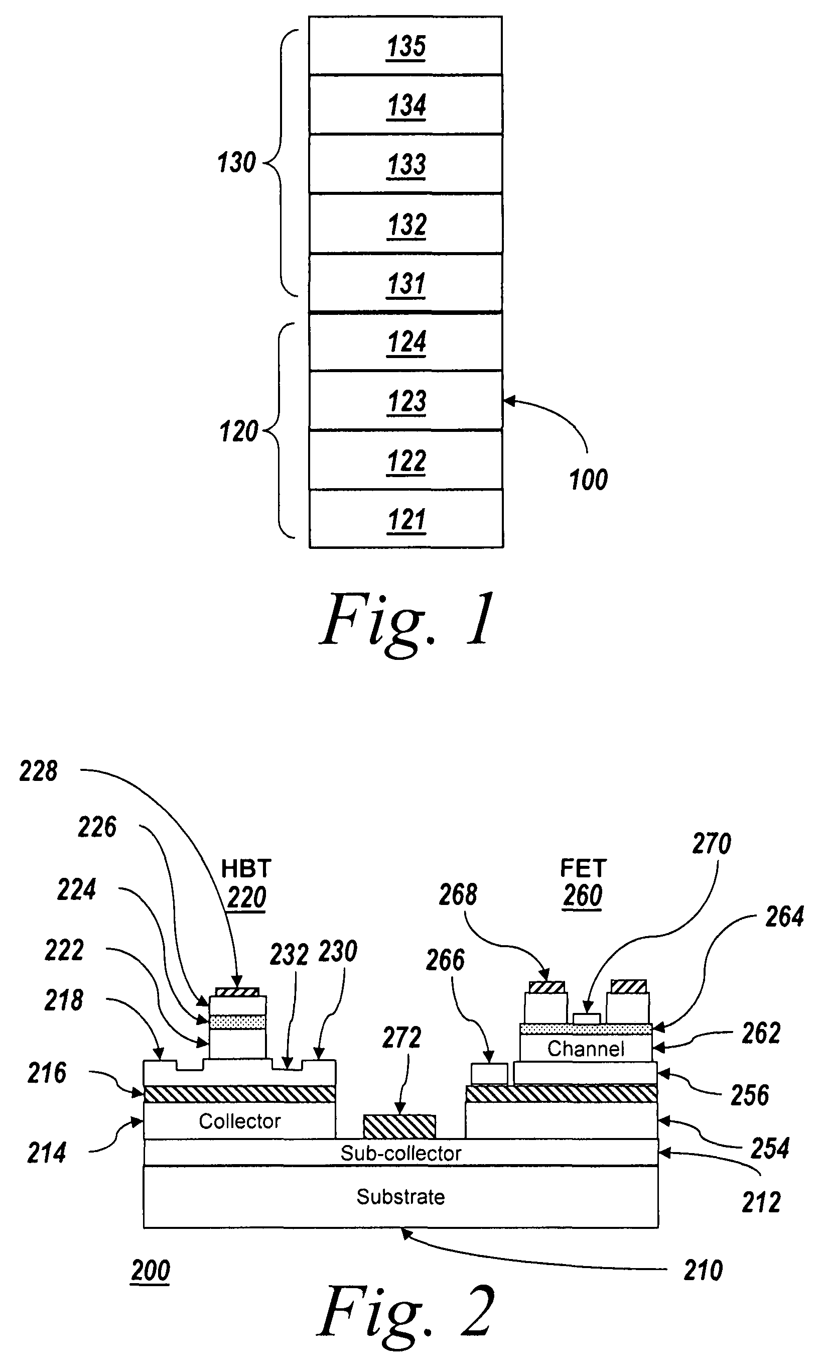
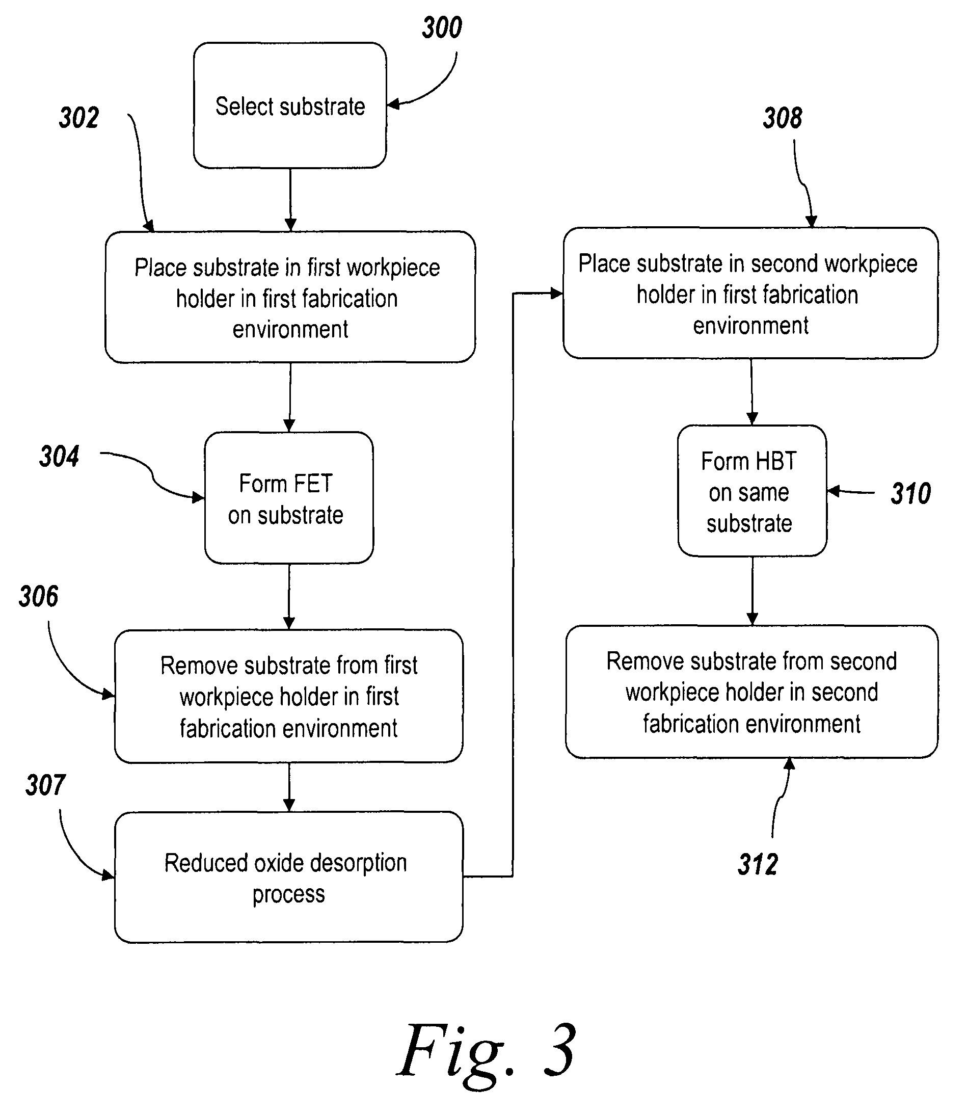
[0029]The present invention discloses fabrication methods for forming and integrated a FET layered structure and an HBT layered structure onto a single common substrate. The FET layered structure and the HBT layered structure are formed in two different fabrication environments on the common substrate. Using this method, a BiFET device may be formed without introducing impurities into the FET portion that detract from the operational characteristics thereof. By separating the growth of the FET device and the HBT device using two or more separate reactors, the operational characteristics for each device forming the BiFET device remain comparable to the operational characteristics of FET devices and HBT devices formed independently and separately on different substrates.

[0030]As used herein, the term “FET” refers to heterostructure field effect transistors (HFET), homogenous field effect transistors (e.g., MESFET, JFET), metal oxide semiconductor FET transistors (MOSFET), high electro...


PUM


Abstract

Methods and systems for fabricating an integrated BiFET using two separate growth procedures are disclosed. Performance of the method fabricates the FET portion of the BIFET in a first fabrication environment. Performance of the method fabricates the HBT portion of the BiFET in a second fabrication environment. By separating the fabrication of the FET portion and the HBT portion in two or more separate reactors, the optimum device performance can be achieved for both devices.

Description

CROSS-REFERENCE TO RELATED APPLICATIONS[0001]This application claims the benefit of and priority from U.S. Provisional Patent Application Ser. No. 60 / 900,009, filed on Feb. 7, 2007, the entire content of which is incorporated herein by reference.BACKGROUND[0002]This invention is related in general to device fabrication and in particular to structures and methods for fabricating an integrated HBT / FET device (a “BiFET”).[0003]Field effect transistors (FETs) and heterojunction bipolar transistors (HBTs) are two common transistor families. The family of FET transistors includes a number of different FET devices having different structures. Members of the FET family include heterostructure field effect transistors (HFET), homogenous field effect transistors (e.g., MESFET, JFET) and metal oxide semiconductor FET transistors (MOSFET).[0004]Devices from the HBT family and the FET family have advantages and disadvantages that render them more suited to certain applications. For instance, HBT...

Claims


Application Information

Patent Timeline
Patent Type & Authority Patents(United States)
IPC IPC(8): H01L21/00
CPCH01L27/0605H01L21/8252H01L21/8249H01L27/0623
Inventor PAN, NORENWIBOWO, ANDREE
Owner MICROLINK DEVICES
Why Eureka
Try Eureka