High frequency switch, amplifying circuit, and mobile communication terminal

a high frequency switch and amplifying circuit technology, applied in the field of high frequency switches, amplifying circuits, mobile communication terminals, can solve the problems of narrow control voltage range, high impedance between the source electrode and the drain electrode, so as to reduce the size of the circuit and simplify the configuration

Inactive Publication Date: 2005-02-08
PANASONIC CORP
View PDF7 Cites 26 Cited by
  • Summary
  • Abstract
  • Description
  • Claims
  • Application Information

AI Technical Summary

Benefits of technology

When the first and second switch elements are composed of field effect transistors, the reference voltage generation circuit comprises a serial circuit of, for example, three or more resistors.
According to this configuratio

Problems solved by technology

This results in a high impedance between the source electrode and the drain electrode of the field effect transistor 132.
This results in a high impedance between the source electrode and the drain electrode of the field effect transistor 131.
A first problem is that in the prior art high frequency switch, the setting range of the control voltage of the high frequency switch depends on the power supply voltage of the high frequency switch, and that the setting range of the control voltage of the high frequency switch is

Method used


Image

  • High frequency switch, amplifying circuit, and mobile communication terminal
  • High frequency switch, amplifying circuit, and mobile communication terminal
  • High frequency switch, amplifying circuit, and mobile communication terminal

Examples


embodiment 1

[Embodiment 1]

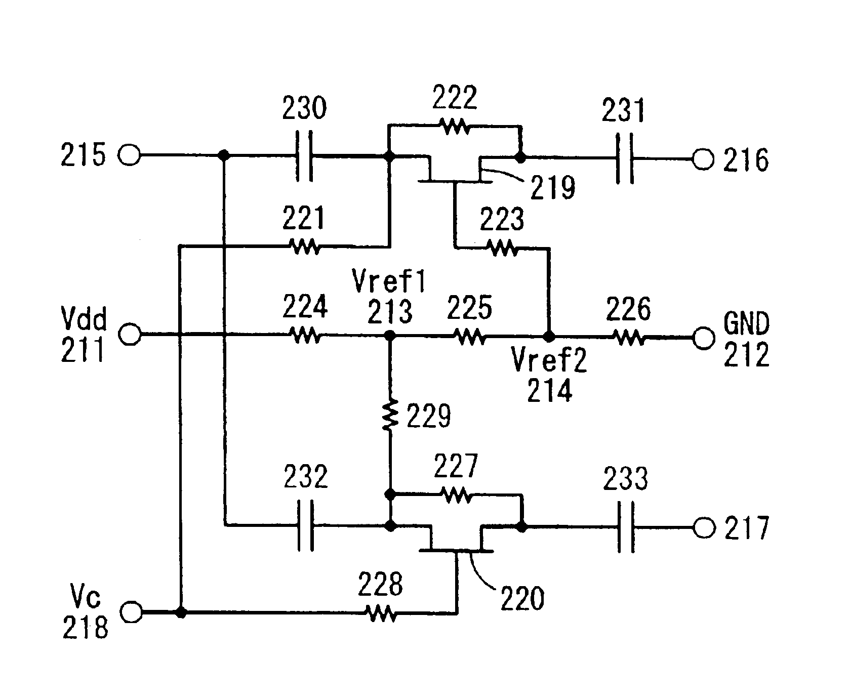
FIG. 1 is a block diagram showing the configuration of a high frequency amplifier circuit according to Embodiment 1 of the invention. The high frequency switch of FIG. 1 is a SPDT switch circuit, and corresponds to the high frequency switch 203 in the block diagram showing the transmitting section of the prior art portable telephone terminal of FIG. 4. That is, in the portable telephone terminal according to the present embodiment of the invention, the high frequency switch of FIG. 1 is used in place of the high frequency switch 203 in the transmitting section of the prior art portable telephone terminal of FIG. 4.

The high frequency switch of FIG. 1 is described below in detail.

In FIG. 1, the source electrode of a field effect transistor 219 serving as a switch element is connected through a capacitor 230 to a signal input terminal 215, while the drain electrode of the field effect transistor 219 is connected through a capacitor 231 to a signal output terminal 216. Fur...

embodiment 2

[Embodiment 2]

FIG. 3 is a block diagram showing the configuration of a high frequency circuit comprising an amplifying circuit according to Embodiment 2 of the invention. The amplifying circuit of FIG. 3 corresponds to the high frequency amplifier circuit 104 and the high frequency switch 105 in the block diagram showing the transmitting section of the prior art portable telephone terminal of FIG. 5. In the portable telephone terminal according to the present embodiment of the invention, the amplifying circuit of FIG. 3 is used in place of the high frequency amplifier circuit 202 and the high frequency switch 203 in the transmitting section 200 of the prior art portable telephone terminal of FIG. 4.

The amplifying circuit of FIG. 3 is described below in detail.

In FIG. 3, a high frequency signal inputted through a signal input terminal 240 is provided through an impedance matching circuit 241 for performing impedance transformation, to a gain control circuit 242, whereby gain attenuat...


PUM


Abstract

In order to provide a high frequency switch in which the setting range of the control voltage is expanded, the high frequency switch is constructed from a switch and a reference voltage generation circuit. The switch comprises first and second field effect transistors. In the first field effect transistor, the source electrode is connected to a signal input terminal, while the drain electrode is connected to a signal output terminal, and while the source electrode is connected to a control terminal. In the second field effect transistor, the source electrode is connected to the signal input terminal, while the drain electrode is connected to the signal output terminal, and while the gate electrode is connected to the control terminal. The reference voltage generation circuit generates two reference voltages the values of which are different from each other, then provides the lower reference voltage to the gate electrode of the first field effect transistor, and then provides the higher reference voltage to the source electrode of the second field effect transistor.

Description

BACKGROUND OF THE INVENTION1. Field of the InventionThe present invention relates to a high frequency switch provided in a high frequency circuit section of a transmitting section of a mobile communication terminal such as a portable telephone terminal and used for switching the signal path of a high frequency signal.The invention further relates to an amplifying circuit for switching the signal path of a high frequency signal and, at the same time, amplifying the high frequency signal.The invention further relates to a mobile communication terminal provided with the high frequency switch or the amplifying circuit mentioned above.In particular, the invention relates to a high frequency switch and an amplifying circuit for switching the signal path of a high frequency signal in response to a control voltage.2. Description of the Related ArtA recent major trend in the field of mobile communication is that a plurality of communication schemes are integrated in an integrated portable te...

Claims


Application Information

Patent Timeline
IPC IPC(8): H03F3/72H03F1/00H03K17/693H03F1/56
CPCH03F1/56H03K17/693H03F3/72H03F2200/429
Inventor NAKAYAMA, MASAOINAMORI, MASAHIKOYAMAMOTO, TAKASHIMOTOYOSHI, KANAME
Owner PANASONIC CORP
Why Eureka
Try Eureka